Multifunctional semiconductor sample fixture

A semiconductor and multi-functional technology, applied in semiconductor/solid-state device manufacturing, electrical components, circuits, etc., can solve the problem of the absence of tiny samples of semiconductor devices, and achieve the effects of avoiding tilt, reducing damage, and avoiding loss

Active Publication Date: 2013-10-09
SHANGHAI HUALI MICROELECTRONICS CORP
View PDF7 Cites 13 Cited by
  • Summary
  • Abstract
  • Description
  • Claims
  • Application Information

AI Technical Summary

Problems solved by technology

[0008] It can be seen that there is currently no special fixture for tiny samples of semiconductor devices.

Method used


Image

  • Multifunctional semiconductor sample fixture
  • Multifunctional semiconductor sample fixture
  • Multifunctional semiconductor sample fixture

Examples


Embodiment Construction

[0044] The invention is a multifunctional semiconductor sample fixture, more specifically a multifunctional fixture used in the micro semiconductor sample testing process.

[0045] A multi-functional semiconductor sample fixture of the present invention is a device applied to the fixation of tiny semiconductor samples. The device can be used as a load-bearing fixture for tiny samples when needles are pricked on a probe station, which is convenient for fixing and increasing the vacuum adsorption of the probe station. It can also be used as a sample holder when small samples are subjected to SEM / FIB analysis.

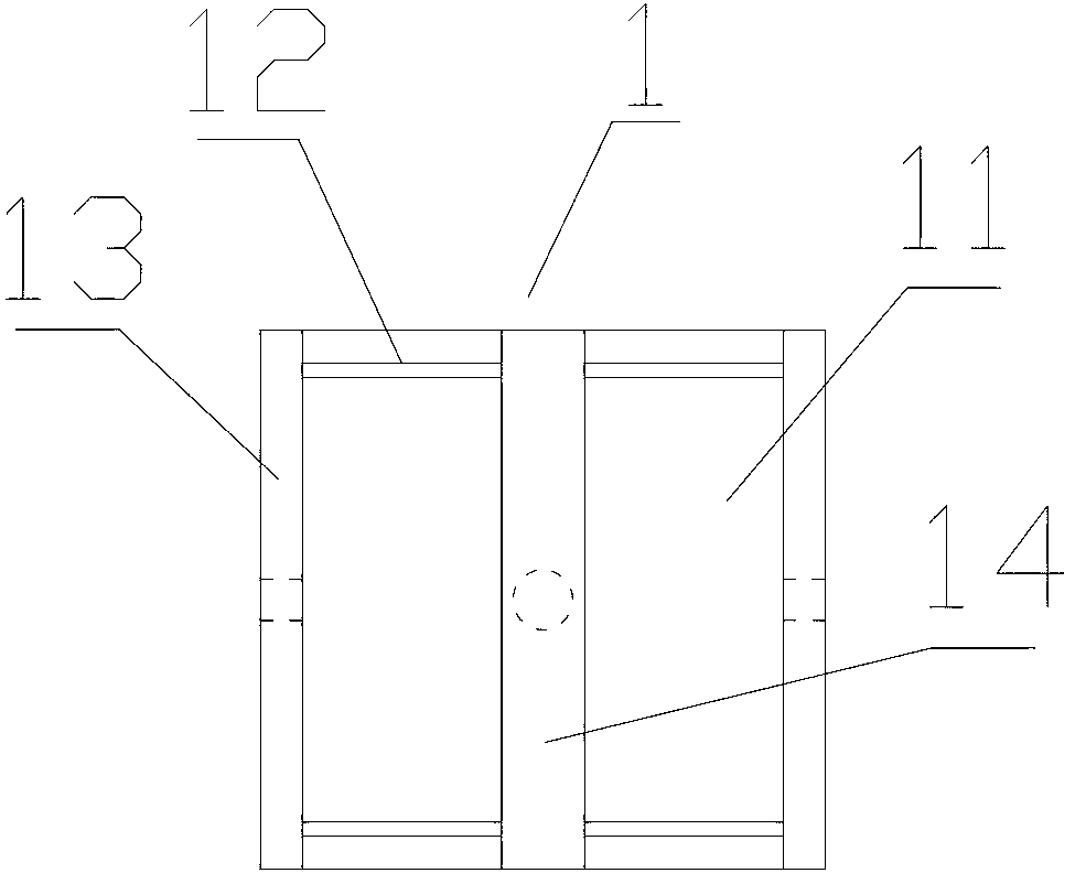
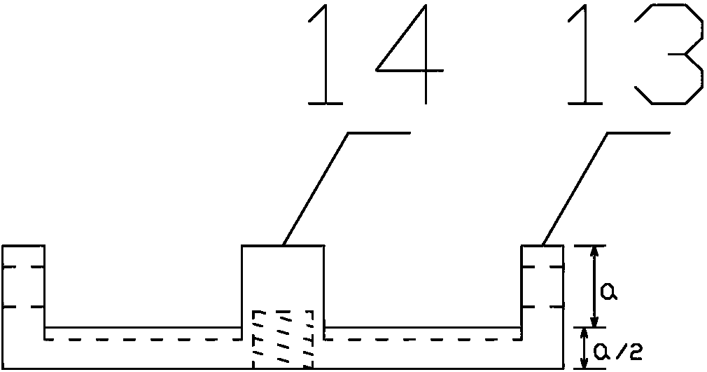
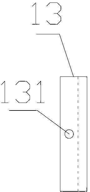
[0046] A multifunctional semiconductor sample holder of the present invention includes a bearing body and a base. A groove and a fixing device are arranged on the carrying body, and the fixing device fixes the semiconductor sample in the groove. The carrying body is also provided with at least three baffles and a bottom plate, and all the baffles are fixedly arranged on ...


PUM


Abstract

The invention relates to a multifunctional semiconductor sample fixture which is used for fixing a semiconductor sample in a testing and analyzing process. A bearing body is provided with a groove and a fixing device. The fixing device is used for fixing the semiconductor sample in the groove. The bearing body is further provided with at least three baffles and a bottom plate. The baffles are all fixedly arranged on the upper surface of the bottom plate. The groove is formed jointly by the two adjacent baffles and the bottom plate between the two baffles. The fixing device comprises a guiding track, a sliding block and a fixing screw rod. The guiding track is arranged on the upper surface of the bottom of the groove, and the guiding direction of the guiding track is perpendicular to the baffles which form the groove. The sliding block moves in a reciprocating mode perpendicular to the baffles through the guiding track. The fixing screw rod is used for fixing the sliding block on the guiding track.

Description

technical field [0001] The invention relates to an auxiliary tool in the processing technology of CMOS semiconductor devices, in particular to a multifunctional fixture applied to tiny samples. Background technique [0002] In the manufacturing and analysis and testing process of semiconductor devices, it is often necessary to perform various processing and analysis on some very small semiconductor samples. Due to the very small size of these samples (usually about 1mm*2mm), it is very inconvenient to transfer and pick and place such tiny samples, and it is also very easy to lose. [0003] For example, when performing ion beam / electron beam (SEM / FIB) dual-beam observation and analysis on tiny samples, it is necessary to stick the sample on the sample holder with conductive adhesive, and press the surface of the sample to fully fix it on the sample holder. The surface of the chip is usually only about a few square millimeters, and it is easy to touch and contaminate the targ...

Claims


Application Information

Patent Timeline
Patent Type & Authority Applications(China)
IPC IPC(8): G01R1/04H01L21/687
Inventor 白月唐涌耀
Owner SHANGHAI HUALI MICROELECTRONICS CORP
Why Eureka
Try Eureka