Method for preparing high In component AlInN thin film

A thin-film, high-temperature technology, used in semiconductor/solid-state device manufacturing, electrical components, circuits, etc., can solve problems such as AlInN composition fluctuation, film quality deterioration, and large lattice mismatch.

Inactive Publication Date: 2013-10-09
INST OF SEMICONDUCTORS - CHINESE ACAD OF SCI
View PDF3 Cites 8 Cited by
  • Summary
  • Abstract
  • Description
  • Claims
  • Application Information

AI Technical Summary

Problems solved by technology

The second is that AlN and InN have large differences in physical properties such as lattice constants and bond lengths, so the grown AlInN is prone to component fluctuations or phase

Method used


Image

  • Method for preparing high In component AlInN thin film
  • Method for preparing high In component AlInN thin film
  • Method for preparing high In component AlInN thin film

Examples


no. 1 example

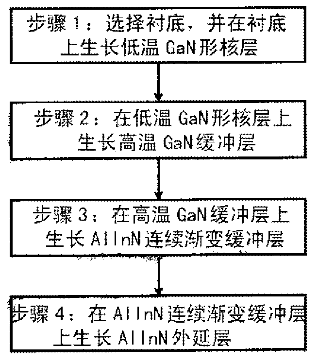
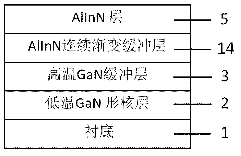
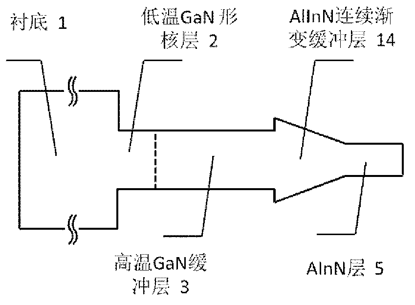
[0030] see figure 1 and figure 2 Shown, the present invention provides a kind of preparation method of high In composition AlInN film, and this method is the first embodiment, comprises the following steps:

[0031] Step 1: grow a low-temperature GaN nucleation layer 2 on a substrate 1, the material of the substrate 1 is sapphire, Si, GaN, SiC or AlN, the thickness of the low-temperature GaN nucleation layer 2 is 20-30nm, and the low-temperature The function of the nucleation layer is mainly to initially release the stress caused by the lattice mismatch between the substrate and the buffer layer;

[0032] Step 2: grow a high-temperature GaN buffer layer 3 on the low-temperature GaN nucleation layer 2. The high-temperature GaN buffer layer 3 has a thickness of 1-3 μm. The high-temperature GaN buffer layer is grown mainly to obtain a smooth film surface, which is the foundation of the subsequent buffer layer. Prepare for growth.

[0033] Step 3: On the high-temperature GaN b...

no. 2 example

[0035] see figure 1 , Figure 4 and Figure 5 As shown, the present invention provides a method for preparing a high In composition AlInN thin film, which is a second embodiment, comprising the following steps:

[0036] Step 1: growing a low-temperature GaN nucleation layer 2 on a substrate 1, the material of the substrate 1 is sapphire, Si, GaN, SiC or AlN, and the thickness of the low-temperature GaN nucleation layer 2 is 20-30nm;

[0037] Step 2: growing a high-temperature GaN buffer layer 3 on the low-temperature GaN nucleation layer 2, and the thickness of the high-temperature GaN buffer layer 3 is 1-3 μm;

[0038] Step 3: growing a multi-layer AlInN composition transition buffer layer 24 on the high temperature GaN buffer layer. The In composition of each layer in the multi-layer AlInN composition transition buffer layer 24 gradually increases from bottom to top, and the bottom In composition is 0.18. This design mainly considers the Al 0.82 In 0.18 N is lattice-mat...


PUM

PropertyMeasurementUnit
Thicknessaaaaaaaaaa
Thicknessaaaaaaaaaa

Abstract

A method for preparing a high In component AlInN thin film comprises the steps of firstly growing a low-temperature GaN nucleation layer on a substrate, secondly, growing a high-temperature GaN buffer layer on the low-temperature GaN nucleation layer, thirdly, growing an AlInN continuous gradient buffer layer on the high-temperature GaN buffer layer and fourthly, growing an AlInN layer on the continuous gradient buffer layer. A novel buffer layer structural design is adopted in the preparation method for the high In component AlInN thin film, stress can be made to be released gradually, the influence of lattice mismatch is reduced, and inducted dislocation in a growing process is reduced.

Description

technical field [0001] The invention belongs to the field of growth of semiconductor nitride materials, and in particular relates to a preparation method of AlInN film with high In composition, mainly adopting three optimized buffer layer structure designs to epitaxial AlInN. Background technique [0002] The ternary alloy material AlInN is a direct bandgap material, and its bandgap width is adjustable from 0.7 to 6.2eV, which is the material with the widest adjustable bandgap range among nitride alloys. At the same time, the AlInN lattice constant also has a large adjustable range. By adjusting the composition ratio, lattice-matched heterostructures such as AlInN / InGaN, AlInN / GaN, and AlInN / AlGaN can be obtained. If it is used as a semiconductor light-emitting device The active layer, whose emission wavelength covers the spectral range from infrared to ultraviolet. Therefore, AlInN materials are widely used in optoelectronic devices such as light-emitting diodes, solar-bli...

Claims


Application Information

Patent Timeline
IPC IPC(8): H01L21/02H01L21/20
Inventor 李维毛德丰王维颖金鹏王占国
Owner INST OF SEMICONDUCTORS - CHINESE ACAD OF SCI
Why Eureka
Try Eureka