Method of measuring conductivity a silicon thin film, method of detecting defects in a silicon thin film, and silicon thin film defect detection device

A technology of silicon thin film and electrical conductivity, which is applied in the direction of measuring devices, measuring electrical variables, testing single semiconductor devices, etc., and can solve the problems of short lifetime of free carriers

Active Publication Date: 2013-10-23
SAMSUNG DISPLAY CO LTD
View PDF9 Cites 17 Cited by
  • Summary
  • Abstract
  • Description
  • Claims
  • Application Information

AI Technical Summary

Problems solved by technology

However, in this technology, the thinner the silicon film, the shorter the free carrier lifetime

Method used


Image

  • Method of measuring conductivity a silicon thin film, method of detecting defects in a silicon thin film, and silicon thin film defect detection device
  • Method of measuring conductivity a silicon thin film, method of detecting defects in a silicon thin film, and silicon thin film defect detection device
  • Method of measuring conductivity a silicon thin film, method of detecting defects in a silicon thin film, and silicon thin film defect detection device

Examples


Embodiment Construction

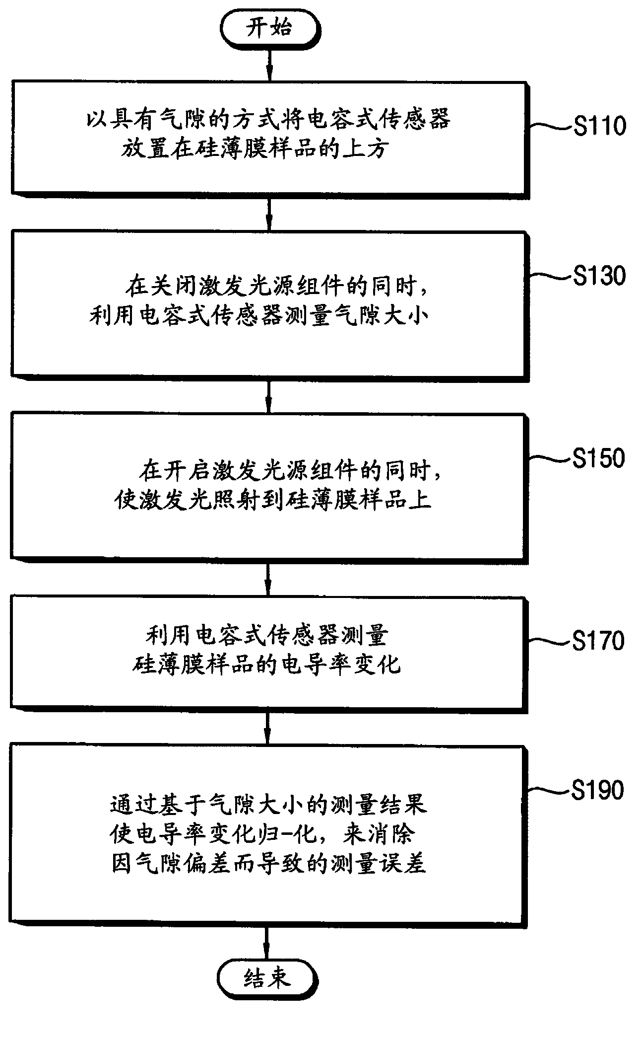
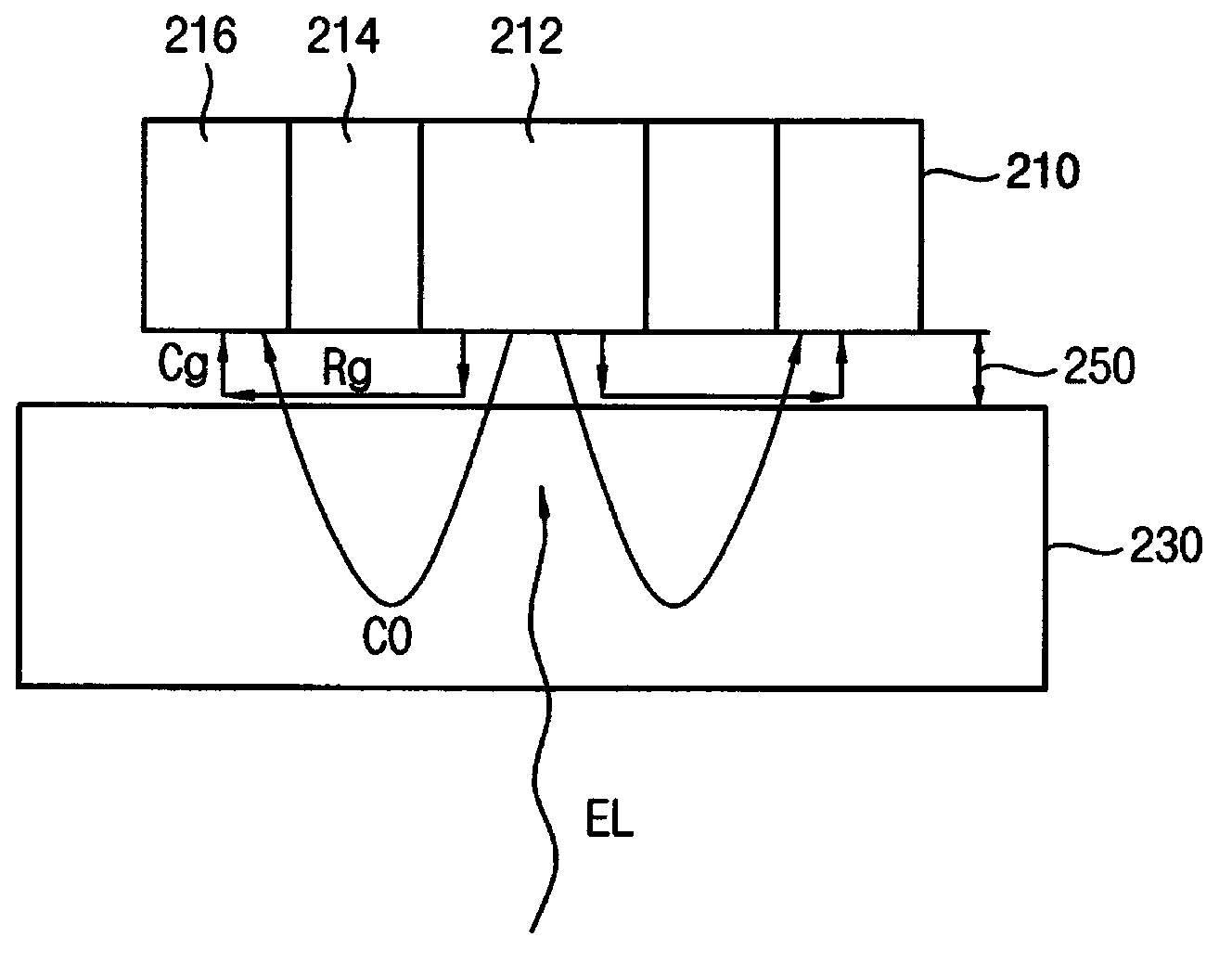
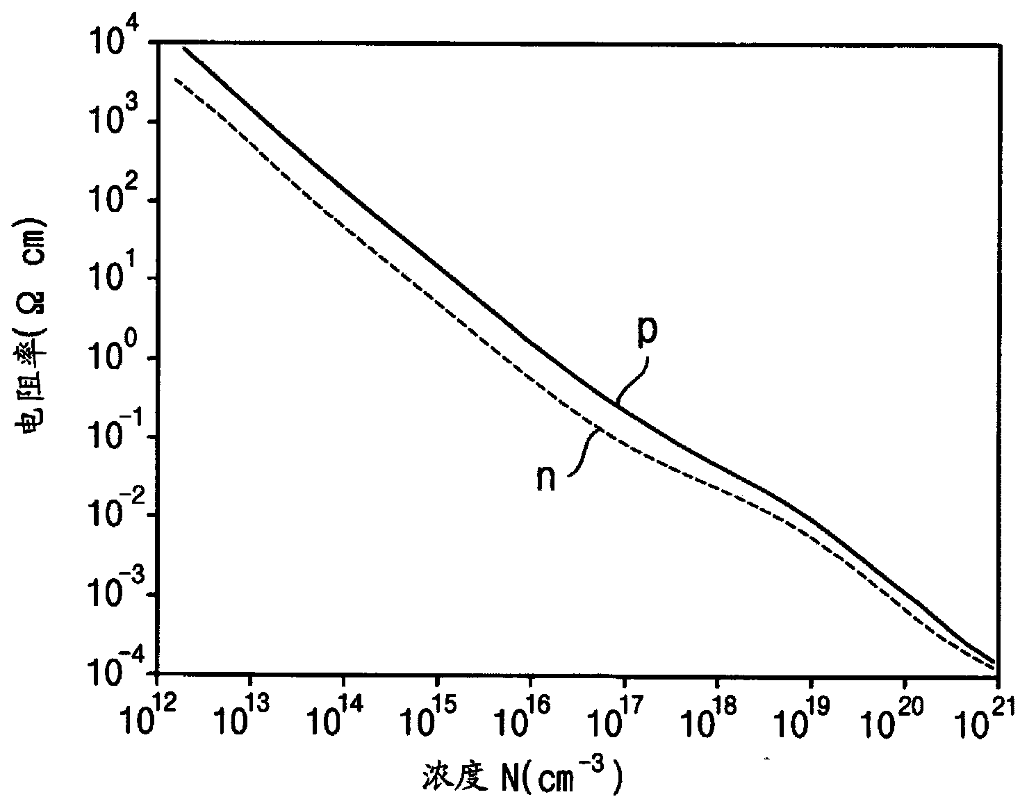
[0044] Various example embodiments will be described more fully hereinafter with reference to the accompanying drawings in which some example embodiments are shown. This invention may, however, be embodied in many different forms and should not be construed as limited to the exemplary embodiments set forth herein. Rather, these example embodiments are provided so that this disclosure will be thorough and complete, and will fully convey the scope of the invention to those skilled in the art. In the drawings, the size and relative sizes of layers and regions may be exaggerated for clarity. Like reference numbers generally refer to like elements throughout.

[0045] It will be understood that, although the terms first, second, third etc. may be used herein to describe various elements, these elements should not be limited by these terms. These terms are used to distinguish one element from another. Thus, a first element discussed below could be termed a second element without ...


PUM

PropertyMeasurementUnit
thicknessaaaaaaaaaa
wavelengthaaaaaaaaaa

Abstract

A method of measuring conductivity of a silicon thin film is provided. By the method, a capacitive sensor is positioned over a silicon thin film sample with an air-gap between the sensor and the sample, a size of the air-gap is measured using the capacitive sensor while an excitation light source module is turned off, an excitation light is illuminated on the silicon thin film sample by turning on the excitation light source module, where the excitation light is an ultraviolet light, a conductivity change of the silicon thin film sample is measured using the capacitive sensor, and a measurement error due to a deviation of the air-gap is eliminated by normalizing the conductivity change based on a measurement result of the size of the air-gap.

Description

[0001] Related Application Cross Reference [0002] This application claims priority from Korean Patent Application No. 10-2012-0036843 filed with the Korean Intellectual Property Office (KIPO) on Apr. 9, 2012, the entire contents of which are hereby incorporated by reference. technical field [0003] Example embodiments relate generally to silicon thin film measurement techniques. More particularly, embodiments of the present invention relate to methods of measuring conductivity of silicon thin films, methods of detecting defects in silicon thin films, and silicon thin film defect detection apparatuses. Background technique [0004] Typically, the quality of thin films is checked using methods for measuring free carrier lifetimes. According to the radio frequency (RF) wave reflection technique, the free carrier lifetime is measured based on the time elapsed for an RF wave impinging on a thin film to return. However, RF wave reflection techniques only measure free carriers...

Claims


Application Information

Patent Timeline
Patent Type & Authority Applications(China)
IPC IPC(8): G01R27/02G01N27/20
CPCG01R31/26G01R31/2648G01R31/265G01N21/63G01N27/24
Inventor 亚历山大·沃罗诺夫李奭浩郑志宪许京会韩圭完
Owner SAMSUNG DISPLAY CO LTD
Why Eureka
Try Eureka