Supercharge Your Innovation With Domain-Expert AI Agents!

Back-side MOM/MIM devices

An oxide and insulator technology, applied in the field of MOM/MIM devices, can solve the problems of increased circuit leakage, low breakdown voltage, reduced circuit performance and reliability, etc.

Active Publication Date: 2013-10-23
GLOBALFOUNDRIES SINGAPORE PTE LTD
View PDF3 Cites 4 Cited by
  • Summary
  • Abstract
  • Description
  • Claims
  • Application Information

AI Technical Summary

Problems solved by technology

However, using larger MOM / MIM wiring leads to an increase in overall chip size and thus higher manufacturing costs
Although thinner dielectric layers can also be utilized in fabricating MOM / MIM devices to achieve higher capacitance, the potential issues with lower breakdown voltage and higher leakage associated with using thinner dielectric layers can lead to overall circuit leakage increase and decrease in circuit performance and reliability

Method used


Image

  • Back-side MOM/MIM devices
  • Back-side MOM/MIM devices
  • Back-side MOM/MIM devices

Examples


Embodiment Construction

[0021] In the following description, for purposes of explanation, numerous specific details are set forth in order to provide a thorough understanding of the exemplary embodiments. It should be apparent, however, that the illustrative embodiments may be practiced without these specific details, or an equivalent arrangement thereof. In other instances, well-known structures and devices are shown in block diagram form in order to avoid unnecessarily obscuring illustrated embodiments. Furthermore, unless otherwise indicated, it is to be understood that all numbers expressing amounts, ratios and numerical characteristics of elements, reaction conditions, etc. used in the specification and claims are modified in all instances by the word "about".

[0022] The present invention addresses and solves the problems of increased chip size and higher manufacturing costs associated with the need for higher capacitance. The present invention addresses and solves such problems, for example,...


PUM


Abstract

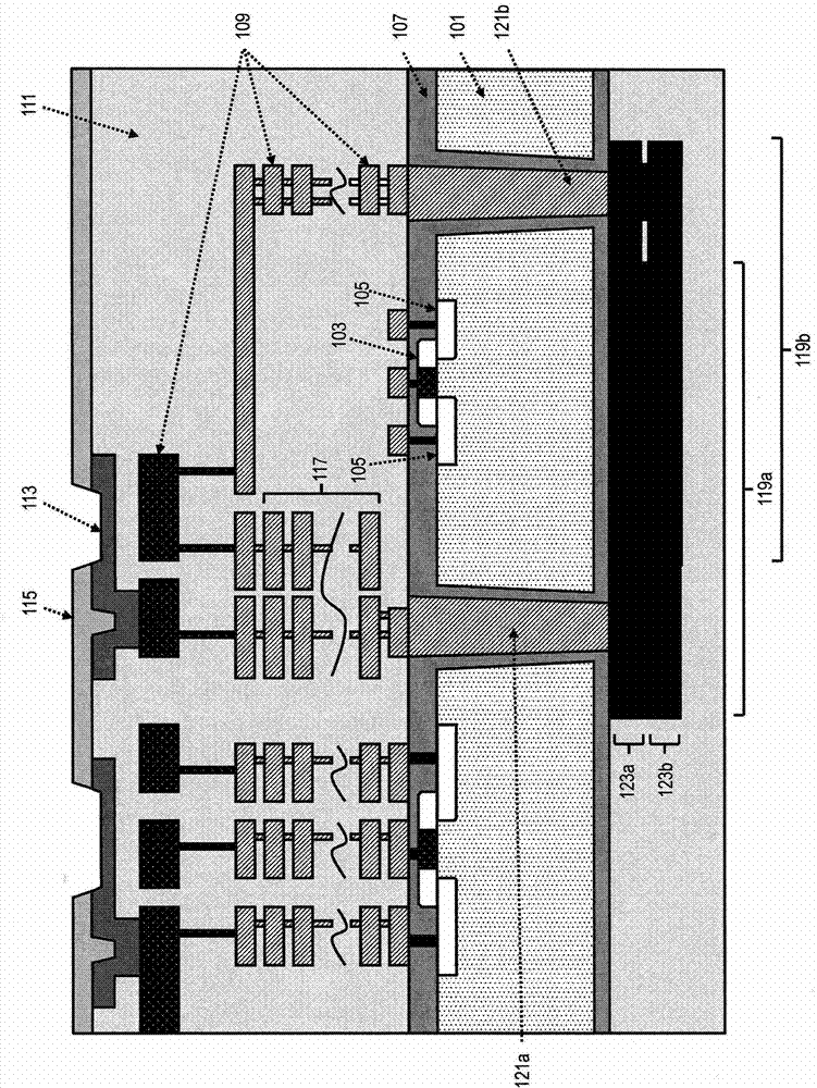
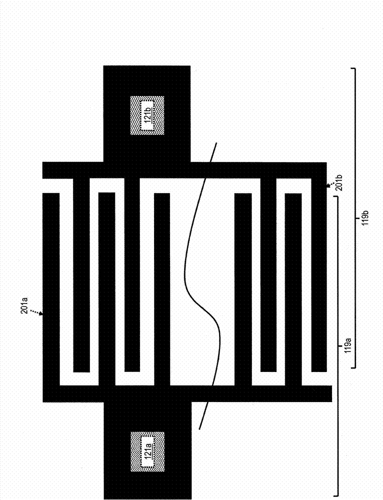
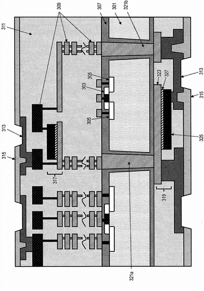
Back-side MOM / MIM structures are integrated on a device with front-side circuitry. Embodiments include forming a substrate having a front side and a back side that is opposite the front side, the substrate including circuitry on the front side of the substrate; and forming a metal-oxide-metal (MOM) capacitor, a metal-insulator-metal (MIM) capacitor, or a combination thereof on the back side of the substrate. Other embodiments include forming a through-silicon via (TSV), in the substrate, connecting the MOM capacitor, the MIM capacitor, or a combination thereof to the circuitry on the front side of the substrate.

Description

technical field [0001] The present invention relates to devices utilizing metal-oxide-metal (MOM) and / or metal-insulator-metal (MIM) capacitors (or circuit systems). The invention is particularly applicable to MOM / MIM devices in semiconductor manufacturing technology. Background technique [0002] Typically, designers will increase the chip area used for MOM / MIM device routing to enable higher capacitance of the MIM / MOM device in its circuit or application. However, using larger MOM / MIM wiring can lead to an increase in overall chip size and thus higher manufacturing costs. Although thinner dielectric layers can also be utilized in fabricating MOM / MIM devices to achieve higher capacitance, the potential issues with lower breakdown voltage and higher leakage associated with using thinner dielectric layers can lead to overall circuit leakage increase and decrease circuit performance and reliability. [0003] Therefore, there is a need for backside MOM / MIM devices and implem...

Claims


Application Information

Patent Timeline
IPC IPC(8): H01L21/768H01L23/522
CPCH01L23/5223H01L23/481H01L21/768H01L2924/0002H01L28/60H01L2924/00
Inventor J·B·谭Y·K·林S·N·袁S·Y·西娅
Owner GLOBALFOUNDRIES SINGAPORE PTE LTD
Features
  • R&D
  • Intellectual Property
  • Life Sciences
  • Materials
  • Tech Scout
  • Unparalleled Data Quality
  • Higher Quality Content
  • 60% Fewer Hallucinations
Learn More