Method for manufacturing silicon wafer markers

A manufacturing method and a technology of marking points, which are applied in the field of solar cells, can solve problems such as damage to silicon wafers, and achieve the effect of reducing the probability of damage

Inactive Publication Date: 2013-10-23
YINGLI GRP
View PDF3 Cites 2 Cited by
  • Summary
  • Abstract
  • Description
  • Claims
  • Application Information

AI Technical Summary

Problems solved by technology

[0004] The present invention aims to provide a method for making marking points on silicon wafers, so as to solve the problem of damage to silicon wafers caused by laser marking points in the prior art

Method used


Image

  • Method for manufacturing silicon wafer markers
  • Method for manufacturing silicon wafer markers

Examples


Embodiment Construction

[0019] It should be noted that, in the case of no conflict, the embodiments in the present application and the features in the embodiments can be combined with each other. The present invention will be described in detail below with reference to the accompanying drawings and examples.

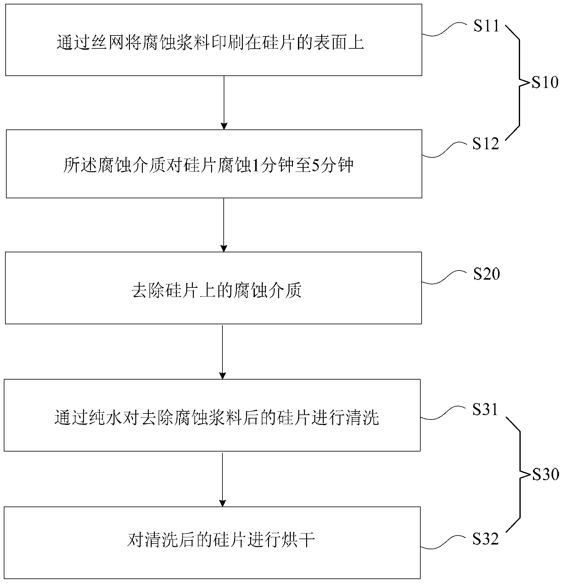
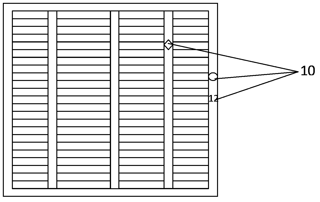
[0020] Such as figure 1 and figure 2 Shown, the manufacturing method of silicon wafer marking point of the present invention comprises the steps:

[0021] Step S10 : performing etching on the silicon wafer to form marking points 10 .

[0022] The manufacturing method of the silicon wafer marking point of the present embodiment forms the marking point 10 at the indicating point on the surface of the silicon wafer by etching. Compared with the laser equipment in the prior art, the marking point 10 is directly processed on the surface of the silicon wafer. The method of manufacturing the marking point 10 will not cause physical damage to the silicon wafer during the manufacturing process, whic...


PUM


Abstract

The invention provides a method for manufacturing silicon wafer markers. The method for manufacturing the silicon wafer markers includes multiple steps, wherein according to the step 10, chemical corrosion is conducted on silicon wafers to form the markers. By the adoption of the mode utilizing corrosion to manufacture the markers, physical damage to the silicon wafers is avoided in the corrosion process, and the probability that the silicon wafers are damaged in the follow-up machining process is reduced.

Description

technical field [0001] The invention relates to the technical field of solar cells, in particular to a method for manufacturing marking points on a silicon wafer. Background technique [0002] In the production process of solar cells, in order to facilitate the tracking of the cells, it is necessary to make marking points on the cells to distinguish them. [0003] In the prior art, marking points on silicon wafers are directly fabricated on silicon wafers by laser equipment. Due to the high power of laser equipment when making marking points, when making marking points on silicon wafers, high temperature will cause physical damage to silicon wafers, resulting in damage to silicon wafers during subsequent processing. Moreover, the cost of the laser equipment is relatively high, and it is not easy to reduce the production cost. Contents of the invention [0004] The invention aims to provide a method for making marking points on silicon wafers, so as to solve the problem i...

Claims


Application Information

Patent Timeline
IPC IPC(8): H01L31/18
CPCY02P70/50
Inventor 王英超熊景峰胡志岩李高非赵文超
Owner YINGLI GRP
Why Eureka
Try Eureka