
Eureka
For R&D, Eureka makes reading and utilizing patents & technical documents easy.
Eureka AIR
Designed for self-driven R&D workflows. Generate viable solutions, solve complex R&D challenges, empower your innovation with AI.

Eureka Materials
Designed for material experts only. Revolutionize your material R&D, from search, analyze, to developing new materials.

TechResearch
Generate reliable direction feasibility study reports for your R&D in just a few steps.

TechSeek
Discover and master advanced knowledge NOW. Basics, ideas, possibilities, all at once.

TechMind
As an expert in R&D Theories, TechMind can generates customized viable solutions instantly.

TechRisk
Analyze your overall solution with one click, know your potential R&D risks in advance.

TechMonitor
Get weekly tech updates, stay abreast of the latest tech innovations and key insights.
Manufacturing method of light emitting diode packaging structure
A technology for light-emitting diodes and packaging structures, which is applied to electrical components, circuits, semiconductor devices, etc., can solve the problems of uneven distribution of phosphors, affecting the light-emitting effect of light-emitting diode packaging structures, etc., and achieve the effects of uniform distribution and simple production process.
- Summary
- Abstract
- Description
- Claims
- Application Information
AI Technical Summary
Problems solved by technology
Method used
Image

Examples
Embodiment Construction
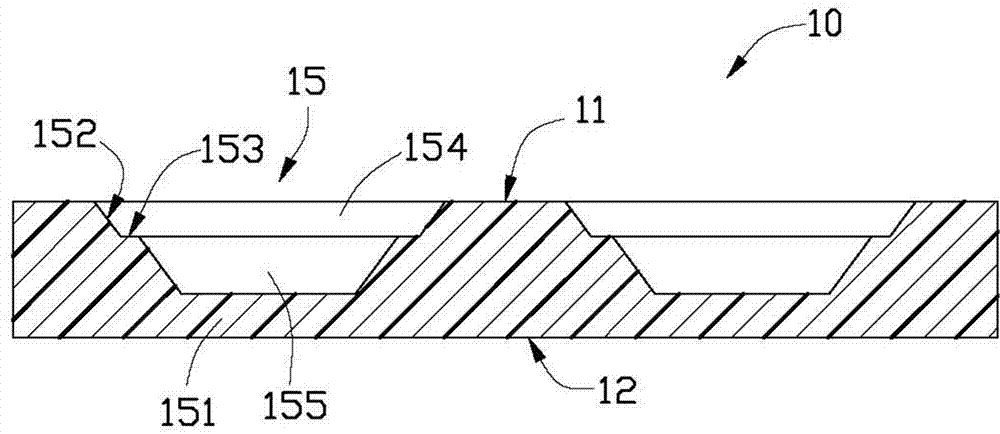
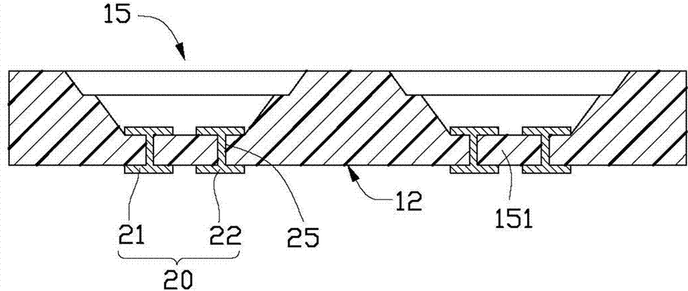
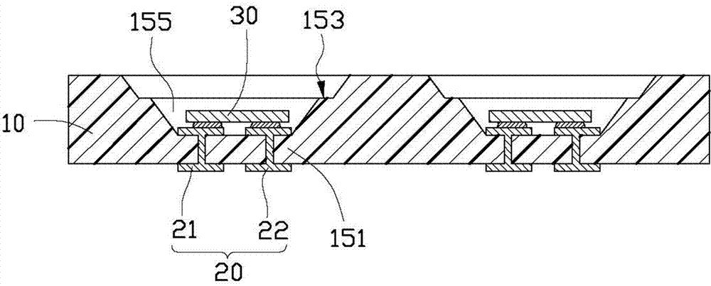
[0018] Such as Figure 7 As shown, the light emitting diode packaging structure 100 provided by the embodiment of the present invention includes a substrate 10, a circuit structure 20 formed on the substrate 10, a light emitting diode chip 30 carried on the substrate 10 and electrically connected to the circuit structure 20, and the packaging structure The fluorescent encapsulation layer 40 of the LED chip 30 .
[0019] In this embodiment, a groove 15 is formed on the substrate 10 , the bottom of the groove 15 is a bottom plate 151 and the surrounding is a side wall 152 . The circuit structure 20 is disposed on the base plate 151 . The light emitting diode chip 30 is accommodated in the groove 15 , and is fixed and electrically connected to the circuit structure 20 of the substrate 10 in a flip-chip manner. The LED chip 30 includes a light emitting surface 31 opposite to the substrate 10 , and two electrodes 32 are disposed on the other surface opposite to the light emitting...
PUM
 Abstract
Description
Claims
Application Information
 - R&D Engineer
- R&D Manager
- IP Professional
- Industry Leading Data Capabilities
- Powerful AI technology
- Patent DNA Extraction
Browse by: Latest US Patents, China's latest patents, Technical Efficacy Thesaurus, Application Domain, Technology Topic, Popular Technical Reports.
© 2024 PatSnap. All rights reserved.Legal|Privacy policy|Modern Slavery Act Transparency Statement|Sitemap|About US| Contact US: help@patsnap.com