A lateral constant current diode
A constant current diode, horizontal technology, applied in the direction of electrical components, circuits, semiconductor devices, etc., can solve the problems of low breakdown voltage, low constant current, etc., and achieve the effect of increasing breakdown voltage, increasing constant current, and easy pinch-off
- Summary
- Abstract
- Description
- Claims
- Application Information
AI Technical Summary
Problems solved by technology
Method used
Image
Examples
Embodiment 1
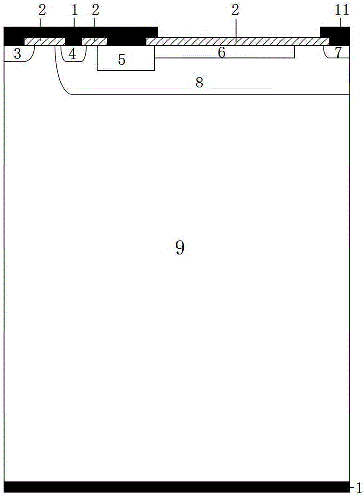
[0033] Such as figure 1 As shown, this example includes a P-type substrate 9, a metalized cathode 1, a metalized anode 11, a first P-type heavily doped region 3 and an N-type well region 8, wherein the first P-type heavily doped region 3 and The N-type well region 8 is respectively arranged between the metallized cathode 1 and the P-type substrate 9 and connected with the metallized cathode 1 and the P-type substrate 9, and the N-type well region 8 includes the first N-type heavily doped region 4, The second P-type heavily doped region 5, the P-type lightly doped region 6 and the second N-type heavily doped region 7, the P-type lightly doped region 6 and the second P-type heavily doped region 5 are connected to form a P-type well region, and the P-type lightly doped region 6 is set on the side of the second P-type heavily doped region 5 close to the second N-type heavily doped region 7, and the metallized cathode 1 covers the first P-type heavily doped region 3 , the top of t...
Embodiment 2
[0039] Such as Figure 4 As shown, in this example, the cathode field plate 12 and the anode field plate 13 are added on the basis of the embodiment 1. The addition of the cathode field plate 12 and the anode field plate 13 can further improve the withstand voltage of the device, and can be based on the actual withstand voltage The lengths of the cathode field plate 12 and the anode field plate 13 need to be adjusted.
Embodiment 3
[0041] This example is a lateral constant current diode with an N-type buffer, such as Figure 5 As shown, specifically, on the basis of Embodiment 1, a buffer layer 10 is added, the buffer layer 10 is arranged between the second N-type heavily doped region 7 and the N-type well region 8, and the concentration of the buffer layer 10 is at the second The doping concentration between the N-type heavily doped region 7 and the N-type well region 8 is used to buffer between the second N-type heavily doped region 7 and the N-type well region 8 to reduce electric field spikes.
PUM
 Abstract
Description
Claims
Application Information


