Transverse constant current diode

A constant current diode, horizontal technology, applied in electrical components, circuits, semiconductor devices, etc., can solve the problems of low constant current and low breakdown voltage, and achieve the effect of increasing constant current, increasing breakdown voltage, and easy pinch-off

Inactive Publication Date: 2013-11-20
UNIV OF ELECTRONICS SCI & TECH OF CHINA
View PDF2 Cites 16 Cited by
  • Summary
  • Abstract
  • Description
  • Claims
  • Application Information

AI Technical Summary

Problems solved by technology

[0003] The technical problem to be solved by the present invention is to propose a new lateral constant current diode for the current constant current diode with low breakdown voltage and low constant current.

Method used


Image

  • Transverse constant current diode
  • Transverse constant current diode
  • Transverse constant current diode

Examples


Embodiment 1

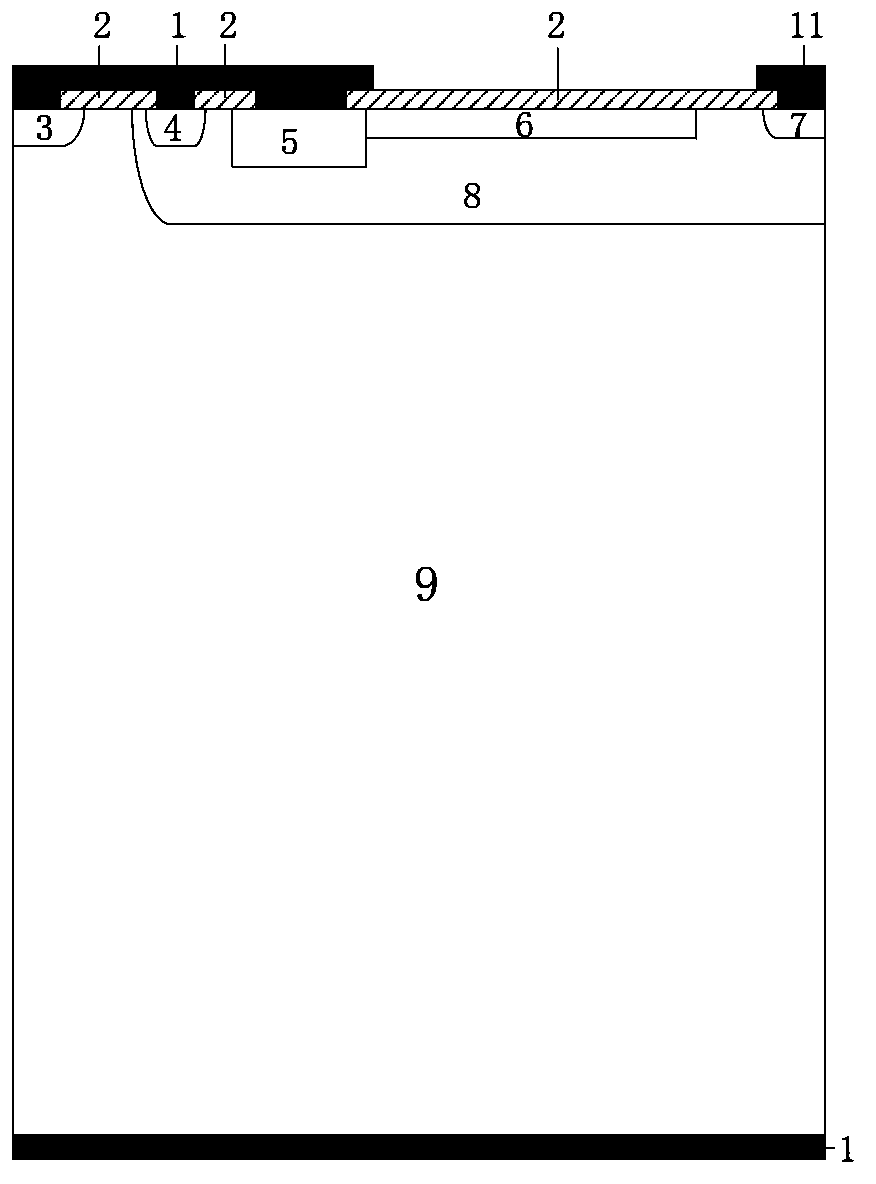
[0033] like figure 1 As shown, this example includes a P-type substrate 9, a metalized cathode 1, a metalized anode 11, a first P-type heavily doped region 3 and an N-type well region 8, wherein the first P-type heavily doped region 3 and The N-type well region 8 is respectively arranged between the metallized cathode 1 and the P-type substrate 9 and connected with the metallized cathode 1 and the P-type substrate 9, and the N-type well region 8 includes the first N-type heavily doped region 4, The second P-type heavily doped region 5, the P-type lightly doped region 6 and the second N-type heavily doped region 7, the P-type lightly doped region 6 and the second P-type heavily doped region 5 are connected to form a P-type well region, and the P-type lightly doped region 6 is set on the side of the second P-type heavily doped region 5 close to the second N-type heavily doped region 7, and the metallized cathode 1 covers the first P-type heavily doped region 3 , the top of the ...

Embodiment 2

[0039] like Figure 4 As shown, in this example, the cathode field plate 12 and the anode field plate 13 are added on the basis of the embodiment 1. The addition of the cathode field plate 12 and the anode field plate 13 can further improve the withstand voltage of the device, and can be based on the actual withstand voltage The lengths of the cathode field plate 12 and the anode field plate 13 need to be adjusted.

Embodiment 3

[0041] This example is a lateral constant current diode with an N-type buffer, such as Figure 5 As shown, specifically, on the basis of Embodiment 1, a buffer layer 10 is added, the buffer layer 10 is arranged between the second N-type heavily doped region 7 and the N-type well region 8, and the concentration of the buffer layer 10 is at the second The doping concentration between the N-type heavily doped region 7 and the N-type well region 8 is used to buffer between the second N-type heavily doped region 7 and the N-type well region 8 to reduce electric field spikes.


PUM


Abstract

The invention relates to semiconductor technologies, and particularly relates to a transverse constant current diode. The transverse constant current diode provided by the invention forms a P-type well region through introducing a lightly doped P-type region and a heavily doped P-type region into an N-type well region, thereby modulating a surface electric field, and improving breakdown voltage. Meanwhile, the lightly doped P-type region can assist to exhaust the N-type well region, thereby enabling a channel to be pinched off more easily, coming into a constant current region quickly, enabling the constant current diode to have lower pinch-off voltage, shortening the channel length of the deep heavily doped P-type region, and improving the constant current of the constant current diode. The transverse constant current diode has the beneficial effects that the breakdown voltage of the transverse constant current diode is improved effectively, the channel is enabled to be pinched off more easily at the same time, the constant current region can be entered quickly, the transverse constant current diode is enabled to have lower pinch-off voltage, and the constant current of the transverse constant current diode is effectively improved. The transverse constant current diode provided by the invention is especially applied to transverse constant current diodes.

Description

technical field [0001] The invention relates to semiconductor technology, in particular to a lateral constant current diode. Background technique [0002] The constant current source is a commonly used electronic equipment and device, and it is widely used in electronic circuits. The constant current source is used to protect the entire circuit, even if the voltage is unstable or the load resistance changes greatly, it can ensure the stability of the supply current. Constant current diodes CRD (Current Regulator Diodes), that is, use diodes as constant current sources to replace ordinary constant current sources composed of multiple components such as transistors, Zener tubes and resistors. At present, the output current of constant current diodes is several milliamperes It can directly drive the load between tens of milliamperes, which realizes the purpose of simplifying the circuit structure, reducing the volume and improving the reliability of the device. In addition, t...

Claims


Application Information

Patent Timeline
Patent Type & Authority Applications(China)
IPC IPC(8): H01L29/861H01L29/06
Inventor 乔明许琬章文通李燕妃何逸涛张昕张波
Owner UNIV OF ELECTRONICS SCI & TECH OF CHINA
Why Eureka
Try Eureka