A vertical constant current diode and its manufacturing method
A constant current diode, vertical technology, used in semiconductor/solid state device manufacturing, electrical components, circuits, etc., to achieve good constant current capability, increase flexibility, and save costs
- Summary
- Abstract
- Description
- Claims
- Application Information
AI Technical Summary
Problems solved by technology
Method used
Image
Examples
Embodiment
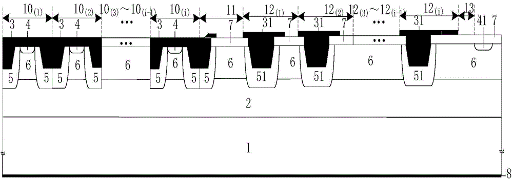
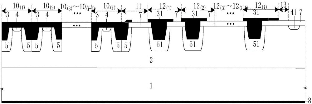
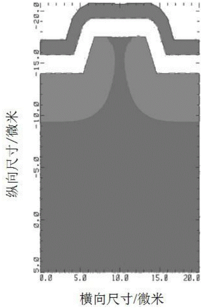
[0058] With the help of MEDICI simulation software provided by figure 1 The vertical constant current diode shown in the process simulation, the simulation parameters are: the initial silicon wafer thickness is about 200μm, the concentration is 1E18cm -3 ; The thickness of the first lightly doped N-type epitaxial layer 2 is about 13 μm, and the concentration is 1E15cm -3 ; The thickness of the second higher doped N-type epitaxial layer 6 is about 6 μm, and the concentration is 4E15cm -3 ; The dose of boron injected is about 4E15cm -3 Form the P+ heavily doped diffusion region 5, and the dose of phosphorus implanted is 4E15cm -3 N + heavily doped 4 is formed. cell 10 (1) 、10 (2). ...10 (6) The widths are equal, each width is about 20 μm, the depth of the P+ heavily doped diffusion region 5 is about 8 μm, and the cell 10 (1) 、10 (2). ...10 (6) The distance between two adjacent P+ heavily doped diffusion regions 5 is equal, about 2 μm. Terminal 12 (1) 、12 (2) 、12 (3)...
PUM
 Abstract
Description
Claims
Application Information


