Jfet device and its manufacturing method

A device, deep well technology, applied in semiconductor/solid-state device manufacturing, semiconductor devices, electrical components, etc., can solve the problems of increased process complexity, high pinch-off voltage, inconvenient adjustment of pinch-off voltage, etc., to achieve low pinch-off voltage, lower doping concentration, easy depletion effect

Active Publication Date: 2020-11-24
SHANGHAI HUAHONG GRACE SEMICON MFG CORP
View PDF6 Cites 0 Cited by
  • Summary
  • Abstract
  • Description
  • Claims
  • Application Information

AI Technical Summary

Problems solved by technology

[0003] The channel region of the existing HV NJFET device is composed of an N-type impurity of DNW104. When DNW104 (source S terminal) and PW105 (gate G terminal) are reverse-biased, DNW104 begins to deplete until the channel region The channel is pinched off by depletion, so the pinch-off voltage is higher
In addition to the high pinch-off voltage, the pinch-off voltage of the existing JFET device is completely determined by the concentration of doping impurities in DNW104, PW105 and substrate 103. As long as the process is certain, the pinch-off voltage is relatively fixed, that is, the pinch-off voltage of the JFET device The adjustment of the pinch-off voltage is inconvenient. When it is necessary to form a variety of JFET devices with different pinch-off voltages on the same wafer substrate, it is necessary to adjust the impurity concentrations of the DNW104, PW105 and the substrate 103 of each device, which will increase the process efficiency. the complexity

Method used


Image

  • Jfet device and its manufacturing method
  • Jfet device and its manufacturing method
  • Jfet device and its manufacturing method

Examples


Embodiment Construction

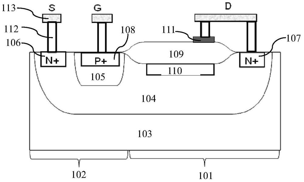
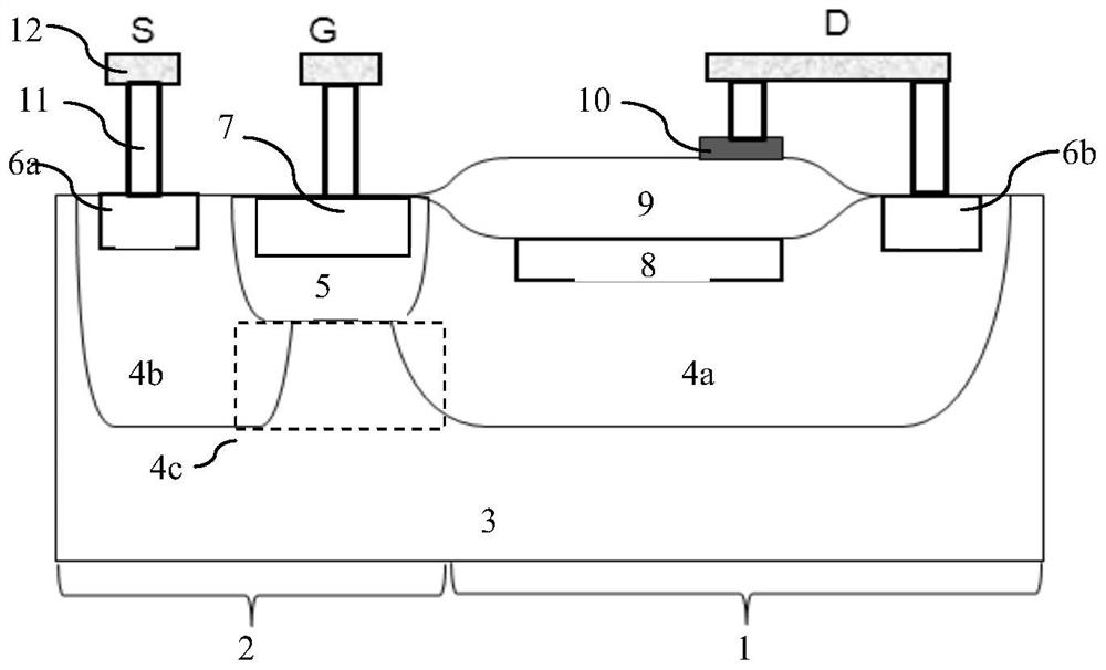
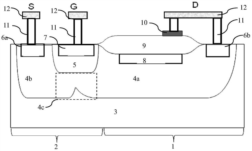
[0038] like figure 2 As shown, it is a cross-sectional view of a JFET device in an embodiment of the present invention before pushing the well; as image 3 As shown, it is a cross-sectional view of a JFET device in Embodiment 1 of the present invention after well pushing; the JFET device in Embodiment 1 of the present invention includes a drift region 1 and a body region 2, and the drift region 1 and the body region 2 are in lateral contact.

[0039] The drift region 1 is composed of a first deep well region 4a doped with a second conductivity type doped on a substrate 3 doped with a first conductivity type; the drain region 6b is formed at the first deep well region 4a The second conductivity type heavily doped region in the selected region; the drain D is drawn out through the contact hole 11 and the metal layer 12 at the top of the drain region 6b.

[0040] The body region 2 includes a second deep well region 4b doped with the second conductivity type and a channel region...


PUM


Abstract

The invention discloses a JFET (junction field-effect transistor) device and a manufacturing method thereof. A drift region is formed by a doped first deep trap region, in a second conduction type, formed on a doped substrate in a first conduction type; a body region comprises a channel region and a doped second deep trap region in the second conduction; the channel region is positioned between the first deep trap region and the second deep trap region and comprises more than two doped third deep trap regions, in the second conduction type, in evenly-spaced arrangement, and doping impurities of a space area between each two adjacent third deep trap regions are formed by diffusion impurities of the adjacent third deep trap region; process conditions of the three deep trap regions are identical. Pinch-off voltage of the JFET device can be adjusted by adjustment of impurity concentration of the deep trap regions, width of each space area and number of the space areas. By the JFET (junction field-effect transistor) device and the manufacturing method thereof, the pinch-off voltage can be lowered, convenience in adjustment of the pinch-off voltage is achieved, and requirements on various different pinch-off voltages can be met.

Description

technical field [0001] The invention relates to the field of semiconductor integrated circuit manufacturing, in particular to a junction field effect transistor (JFET) device. The invention also relates to a manufacturing method of the JFET device. Background technique [0002] like figure 1 As shown, it is a cross-sectional view of an existing JFET device. Taking a high-voltage (HV) N-type channel JFET device as an example, the description is as follows: HV NJFET devices generally consist of two parts, one part is the drift region 101 at the drain (Drain) end, and the other part is the body region 102 . The drift region 102 mainly serves the purpose of high voltage resistance. Because of the need for high voltage resistance, a deep (Deep) and relatively light N well (NW), namely DNW104, is required. The DNW104 is formed in the P-type substrate 103. However, since DNW104 cannot be too light, it will affect the on-resistance, so it needs to be made relatively thicker, and ...

Claims


Application Information

Patent Timeline
Patent Type & Authority Patents(China)
IPC IPC(8): H01L29/808H01L21/337H01L29/06H01L21/265
Inventor 宁开明金锋
Owner SHANGHAI HUAHONG GRACE SEMICON MFG CORP
Why Eureka
Try Eureka