Eureka AIR delivers breakthrough ideas for toughest innovation challenges, trusted by R&D personnel around the world.

Method for producing AlGaN/AlInN composite potential barrier gallium nitride field effect pipe

A compound barrier and gallium nitride field technology, applied in the field of semiconductor devices, can solve problems such as difficulty in forming electron gas density and failure to manufacture high-power field effect transistors, so as to suppress current collapse and solve short channel effects , Improve the effect of electron gas density

Inactive Publication Date: 2009-12-16
NO 55 INST CHINA ELECTRONIC SCI & TECHNOLOGYGROUP CO LTD
View PDF2 Cites 0 Cited by
  • Summary
  • Abstract
  • Description
  • Claims
  • Application Information

AI Technical Summary

Problems solved by technology

However, the barrier of the single-barrier heterostructure is very thin, and it is difficult to form a perfect channel well to accommodate such a large electron gas density
So far, no high-power field effect transistors have been produced

Method used


Image

  • Method for producing AlGaN/AlInN composite potential barrier gallium nitride field effect pipe
  • Method for producing AlGaN/AlInN composite potential barrier gallium nitride field effect pipe
  • Method for producing AlGaN/AlInN composite potential barrier gallium nitride field effect pipe

Examples


Embodiment 1

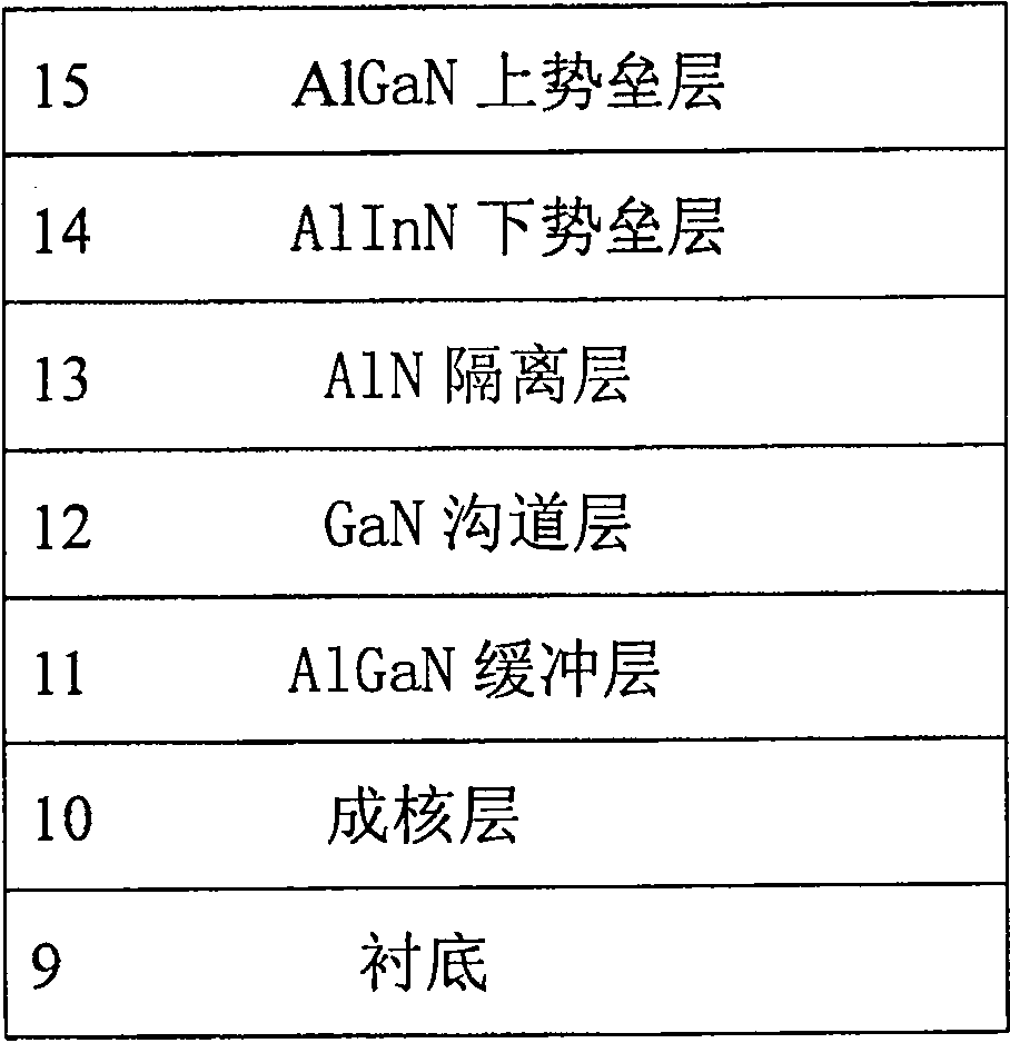
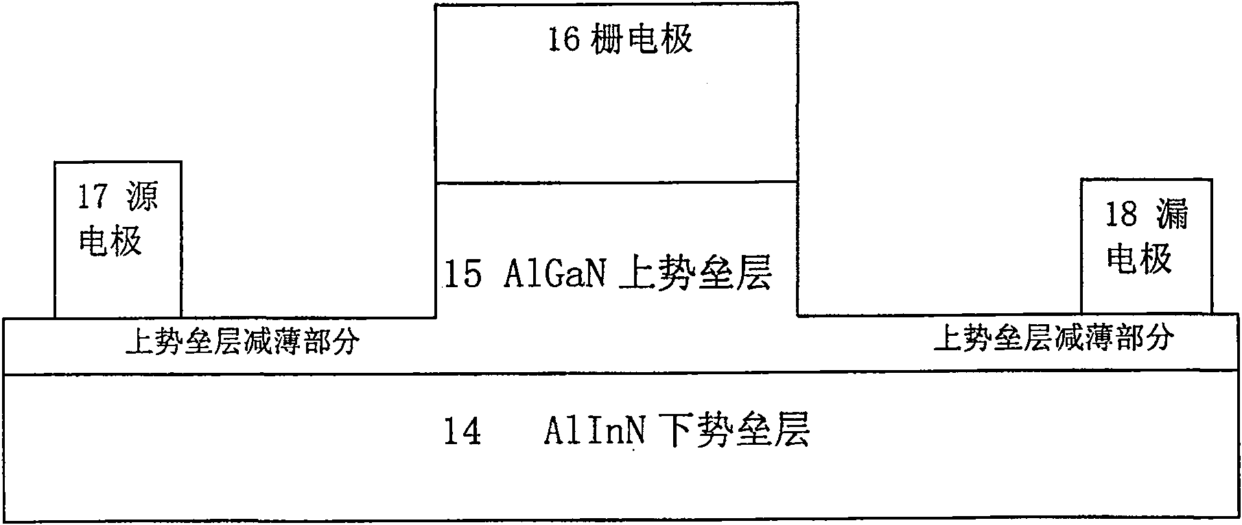
[0019] Select low aluminum (Al) composition ratio alloy Al 0.04 Ga 0.96 N is the buffer layer 11, grow 15nm undoped GaN as channel layer 12, and then grow 2nm undoped AlN isolation layer 13 and 4nm undoped Al on it 0.83 In 0.17 N lower barrier layer 14, finally covered with 6nm undoped Al 0.3 Ga 0.7 N upper barrier layer 15 . Self-consistently solving the Schrödinger equation and Poisson equation, the channel electron gas density is 15.29×10 12 cm -2 , the pinch-off voltage is -4V. When the thinned Al 0.3 Ga 0.7 When the barrier layer on N is 2nm, the calculated electron gas density is 1.696×10 13 cm -2 . After making the ohmic electrode through the superalloy, the Al formed under the source electrode 17 and the drain electrode 18 0.83 In 0.17 The N / AlN / GaN heterojunction electron gas density is as high as 2.96×10 13 m -2 . Greatly reduced ohmic contact resistance.

Embodiment 2

[0020] Embodiment 2: choose low aluminum (Al) composition ratio alloy Al 0.04 Ga 0.96N is the buffer layer 11, grow 15nm undoped GaN as channel layer 12, and then grow 2nm undoped AlN isolation layer 13 and 4nm undoped Al on it 0.83 In 0.17 The lower N barrier layer 14 finally covers the upper barrier layer 15 of 6nm undoped GaN. Self-consistently solving the Schrödinger equation and Poisson equation, the channel electron gas density is 9.097×10 12 m -2 , the pinch-off voltage is -2.8V. When the thinned GaN upper barrier layer is 2nm, the calculated electron gas density is 13.645×10 12 cm -2 . Thinning the barrier increases the electron gas density by 4.55×10 12 cm -2 , significantly weakening the strong field peak in the channel. After making the ohmic electrode through the superalloy, the Al formed under the source electrode 17 and the drain electrode 18 0.83 In 0.17 The N / AlN / GaN heterojunction electron gas density is as high as 2.96×10 13 cm -2 . Greatly red...

Embodiment 3

[0021] Embodiment 3: choose low aluminum (Al) composition ratio alloy Al 0.04 Ga 0.96 N is the buffer layer 11, grow 15nm undoped GaN as channel layer 12, and then grow 2nm undoped AlN isolation layer 13 and 4nm undoped Al on it 0.83 In 0.17 N lower barrier layer 14, finally covered with 5nm undoped Al 0.1 Ga 0.9 N upper barrier layer 15 . Self-consistently solving the Schrödinger equation and Poisson equation, the channel electron gas density is 11.56×10 12 cm -2 , the pinch-off voltage is -2.8V. When the thinned Al 0.1 Ga 0.9 When the barrier layer on N is 2nm, the calculated electron gas density is 1.457×10 13 cm -2 . Thinning the potential barrier increases the electron gas density by 3.01×10 12 m -2 , significantly weakening the strong field peak in the channel. After making the ohmic electrode through the superalloy, the Al formed under the source electrode 17 and the drain electrode 18 0.83 In 0.17 The N / AlN / GaN heterojunction electron gas density is as ...


PUM

PropertyMeasurementUnit
thicknessaaaaaaaaaa
thicknessaaaaaaaaaa
thicknessaaaaaaaaaa

Abstract

The invention is a method for manufacturing AlGaN / AlInN compound barrier gallium nitride field effect transistor. The process steps are divided into sequentially growing a nucleation layer, an AlGaN buffer layer, a GaN channel layer, an AlN isolation layer and an AlInN layer on a substrate. The lower barrier layer; the AlGaN upper barrier layer is covered on the AlInN lower barrier layer to form a composite barrier; the AlGaN upper barrier layer on the AlGaN upper barrier layer is thinned except for the area reserved for gate electrodes by microelectronic technology Layer; making source electrode and drain electrode on the thinned part; making gate electrode on the area reserved for making gate electrode on the AlGaN upper barrier layer. Advantages: broaden and increase the potential barrier, improve the channel well structure, enhance the two-dimensional characteristics of the electron gas, and the strong negative polarized charge on the AlGaN / AlInN heterointerface increases the strength of energy band clipping, and meets the requirements of ohmic contact and Schottky potential different heterostructure requirements throughout the barrier, under-gate trench, and off-gate trench.

Description

technical field [0001] The invention relates to a method for manufacturing an AlGaN / AlInN compound barrier gallium nitride field effect transistor with low defect density, high current and high reliability. It belongs to the technical field of semiconductor devices. Background technique [0002] The strong polarized charge and large energy band order on the AlGaN / GaN heterointerface generate a high-density two-dimensional electron gas, which improves the output power of GaN field effect transistors by an order of magnitude compared with GaAs field effect transistors. However, when the Al composition ratio of the barrier layer is increased to increase the channel electron gas density, the lattice mismatch increases, a large number of defects are introduced, and the device performance decreases rapidly. The currently used Al composition ratios are all below 0.35, which limits the band-cutting range of the heterojunction. Each part of the field effect tube has different requi...

Claims


Application Information

Patent Timeline
Patent Type & Authority Patents(China)
IPC IPC(8): H01L21/335
Inventor 薛舫时
Owner NO 55 INST CHINA ELECTRONIC SCI & TECHNOLOGYGROUP CO LTD
Why Eureka
Eureka Blog
Learn More