A junction field effect transistor

A technology of field effect transistors and junctions, applied in semiconductor devices, electrical components, circuits, etc., can solve the problems of high current conduction capacity, small pinch-off voltage, and JFET cannot be guaranteed at the same time, and achieve high drain-source breakdown voltage , the effect of uniform electric field distribution

Active Publication Date: 2017-12-22
FOUNDER MICROELECTRONICS INT
View PDF3 Cites 0 Cited by
  • Summary
  • Abstract
  • Description
  • Claims
  • Application Information

AI Technical Summary

Problems solved by technology

[0009] The present invention provides a junction field effect transistor, which is used to solve the problem of increasing the doping concentration of the channel in the existing JFET structure and improving the current conduction capability, the pinch-off voltage of the device is also larger, and the drain-source breakdown voltage is lower. The smaller the JFET, the higher the current conduction capability, the drain-source breakdown voltage, and the smaller pinch-off voltage cannot be guaranteed at the same time.

Method used


Image

  • A junction field effect transistor
  • A junction field effect transistor

Examples


Embodiment Construction

[0022] The specific implementation manners of the present invention will be further described in detail below in conjunction with the accompanying drawings and embodiments. The following examples are used to illustrate the present invention, but are not intended to limit the scope of the present invention.

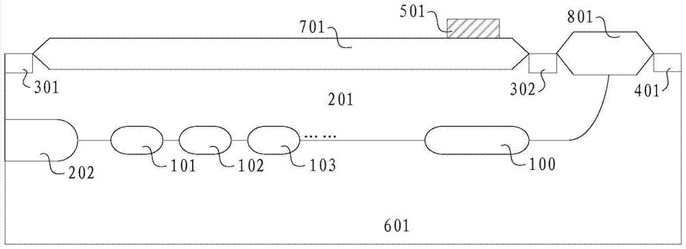
[0023] Such as figure 2 As shown, the embodiment of the present invention provides a junction field effect transistor, which includes a P-type substrate 601 and a first N-type lightly doped region 201 located in the upper surface layer of the P-type substrate 601 . The first N-type lightly doped region 201 serves as the channel of the JFET. Specifically, the doping concentration of the first N-type lightly doped region 201 can be set to be greater than the doping concentration of the P-type substrate 601 . A first N-type heavily doped region 301 and a second N-type heavily doped region 302 are formed in the upper surface layer at both ends of the first N-type lightly do...


PUM


Abstract

The invention belongs to the semiconductor device field and discloses a junction field effect transistor. According to the junction field effect transistor, a back grid is formed between a trench and a P substrate of the JFET (junction type field effect transistor) and is corresponding to the position of a positive grid, and as a result, when negative voltage is applied to the grids, depletion regions of a positive grid PN junction and a negative grid PN junction do not horizontally extend, but vertically extend with the increase of the negative voltage, so that small pinch-off voltage can be obtained; drain-source voltage is mainly borne by horizontal extension of the depletion regions, and P type lightly-doped regions which are adjacent to a source are formed between the trench and the P substrate of the JFET, so that the distribution of an electric field in the trench of the JFET is more uniform, and N type lightly-doped regions which are located below a drain are formed between the trench and the P substrate of the JFET, and thus, breakdown of a PN junction formed by the trench and the P substrate of the JFET, which occurs at the bottom of a drain end, can be avoided, and as a result, high drain-source breakdown voltage can be obtained. With the junction field effect transistor adopted, contradictions among three parameters, namely, the pinch-off voltage, the drain-source breakdown voltage and current conduction capacity, can be alleviated.

Description

technical field [0001] The invention relates to the field of semiconductor devices, in particular to a junction field effect transistor. Background technique [0002] Junction Field Effect Transistor (JFET for short) is one of the most common semiconductor devices, including N-channel Junction Field Effect Transistor and P-channel Junction Field Effect Transistor. In practical applications, commonly used It is an N-channel JFET (hereinafter, JFET refers to N-channel JFET). [0003] The basic structure of N-channel JFET is to diffuse two P-type doped regions on both sides of the N-type semiconductor to form two PN junctions. These two P-type doped regions are the gates of the JFET. The N-type semiconductor region between the doped regions is the channel of the JFET, and the two ends of the N-type semiconductor are respectively the source and the drain of the JFET. figure 1 Shown is a common JFET structure such as figure 1 As shown, the N-type lightly doped region 10 is for...

Claims


Application Information

Patent Timeline
Patent Type & Authority Patents(China)
IPC IPC(8): H01L29/423H01L29/06H01L29/808
CPCH01L29/1066H01L29/42316H01L29/808
Inventor 潘光燃石金成高振杰文燕王焜
Owner FOUNDER MICROELECTRONICS INT
Why Eureka
Try Eureka