Structure and Fabrication Method of High Voltage Junction Field Effect Transistor

A field effect transistor and junction technology, which is applied to the structure of high-voltage junction field effect transistors and the field of preparation thereof, can solve the problems of high impurity concentration and high device pinch-off voltage, and achieves lower impurity concentration, lower pinch-off voltage, and easy depleted effect

Active Publication Date: 2015-10-14
SHANGHAI HUAHONG GRACE SEMICON MFG CORP
View PDF3 Cites 0 Cited by
  • Summary
  • Abstract
  • Description
  • Claims
  • Application Information

AI Technical Summary

Problems solved by technology

[0005] The HV JFET device with this structure, because its body region channel is only composed of a single impurity (N-type or P-type), that is, the concentration of the impurity is relatively high, and the channel path is not easy to be depleted. Therefore, the pinch-off voltage of the device will be higher

Method used


Image

  • Structure and Fabrication Method of High Voltage Junction Field Effect Transistor
  • Structure and Fabrication Method of High Voltage Junction Field Effect Transistor
  • Structure and Fabrication Method of High Voltage Junction Field Effect Transistor

Examples


Embodiment Construction

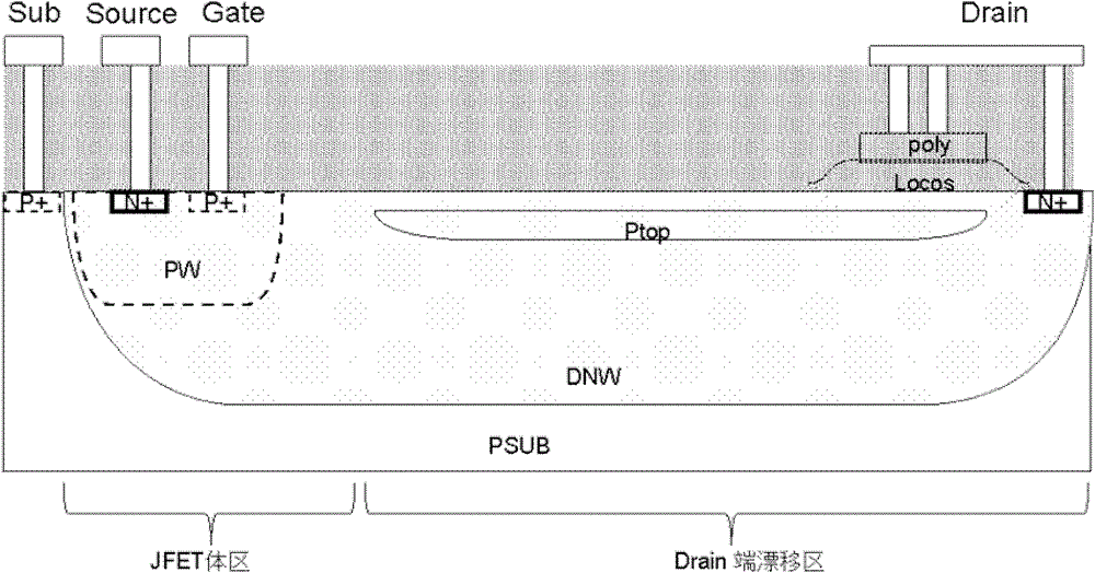
[0024] In order to have a more specific understanding of the technical content, characteristics and efficacy of the present invention, now taking the HV JFET of N-type channel as an example, combined with the illustrated embodiment, the technical solution of the present invention is described in detail as follows:

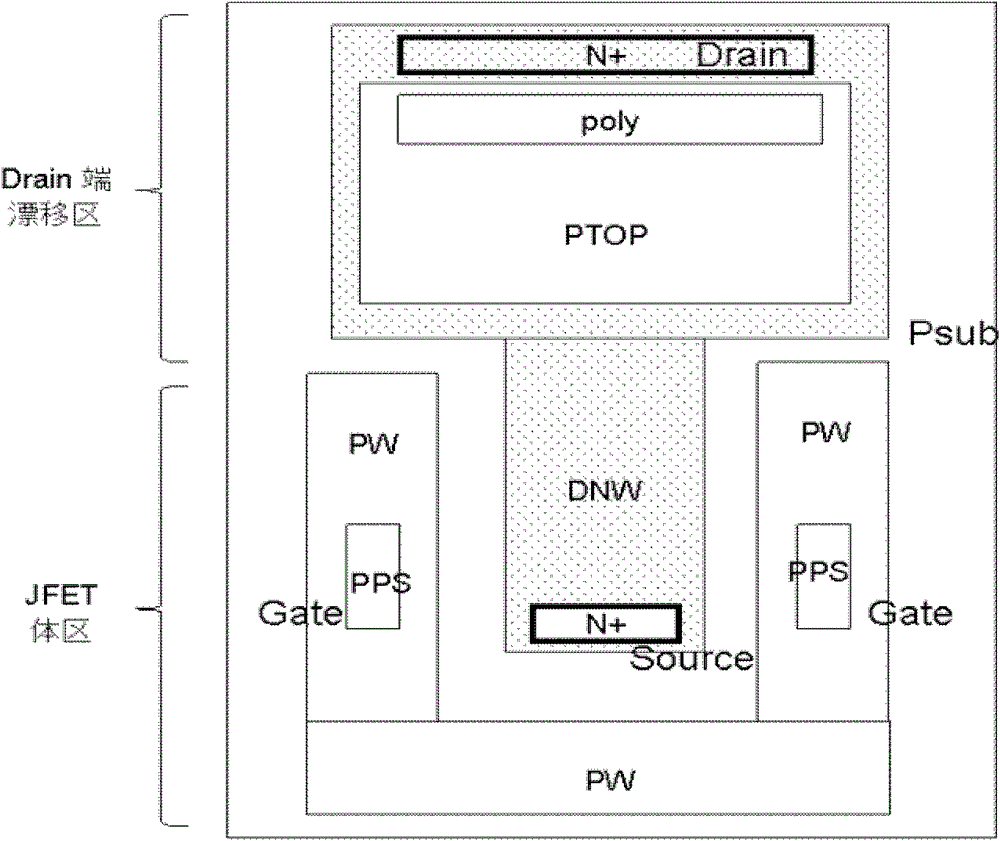
[0025] The structure of the HV NJFET of this embodiment is as Figures 4 to 6 As shown, in addition to injecting Ptop into the DNW of the drain drift region, Ptop is also injected into the DNW of the body region. The specific preparation process of the HV NJFET device with this structure is as follows:

[0026] Step 1, on a low-doped P-type substrate (PSUB), use a photolithography process and an ion implantation process to form the DNW of the drain end drift region and the JFET body region.

[0027] In step 2, PW is formed on a low-doped P-type substrate by using a photolithography process and an ion implantation process. The PW can surround the DNW of the JFET b...


PUM


Abstract

The invention discloses a high-voltage junction field effect transistor structure. An inversion layer is filled into a deep channel of a body region of the structure. The invention further discloses a manufacture method of the high-voltage junction field effect transistor structure (HV JFET) structure. The manufacture method comprises the steps of manufacturing the inversion layer in the deep channel of the body region through a photoetching and ion implantation process while manufacturing a substrate trap of a manufacture body region or the inversion layer of a drain terminal drifting region in the HV JFET conventional manufacture process. By filling one opposite type of impurities into the deep channel of the JFET body region, the impurity concentration of the channel of the JFET body region is reduced on a basis that any photoetching layer is not increased, the channel is easily used up, and accordingly the pinch-off voltage of an HV JFET device is effectively reduced.

Description

technical field [0001] The invention relates to the field of semiconductor integrated circuit manufacturing, in particular to a structure of a high-voltage junction field effect transistor and a preparation method thereof. Background technique [0002] The traditional high-voltage junction field effect transistor (High-Voltage Junction Field Effect Transistor, HVJFET) generally consists of two parts, the Drain (drain) end drift region and the JFET body region, such as figure 1 shown. in, [0003] The drain drift region mainly plays the role of high voltage resistance, and has a DNW (N-type deep well). Since the N-type impurity concentration in DNW is too light, it will affect the on-resistance, so it needs to be made relatively thicker, and an additional layer of inversion implantation is added, such as figure 1 In the Ptop (P-type buried layer), to balance its charge. [0004] The body region is mainly used to control the magnitude of the JFET current and the pinch-off ...

Claims


Application Information

Patent Timeline
Patent Type & Authority Patents(China)
IPC IPC(8): H01L29/36H01L29/808H01L21/266H01L21/337
Inventor 宁开明董科
Owner SHANGHAI HUAHONG GRACE SEMICON MFG CORP
Why Eureka
Try Eureka