Semiconductor device

a technology of mikro-conductor and body, applied in the direction of mikro-conductor devices, basic electric elements, electrical equipment, etc., can solve the problem that the region in the drift layer sandwiched between the buffer layer and the body region is not fully utilized as a current flow path, and achieve the effect of reducing on-resistan

Inactive Publication Date: 2012-11-22
SUMITOMO ELECTRIC IND LTD
View PDF2 Cites 22 Cited by
  • Summary
  • Abstract
  • Description
  • Claims
  • Application Information

AI Technical Summary

Benefits of technology

[0006]The present invention was made to solve such problems, and an object of the present in

Problems solved by technology

In a conventional vertical semiconductor device, a region in the drift layer sandwiched b

Method used


Image

  • Semiconductor device
  • Semiconductor device
  • Semiconductor device

Examples


Embodiment Construction

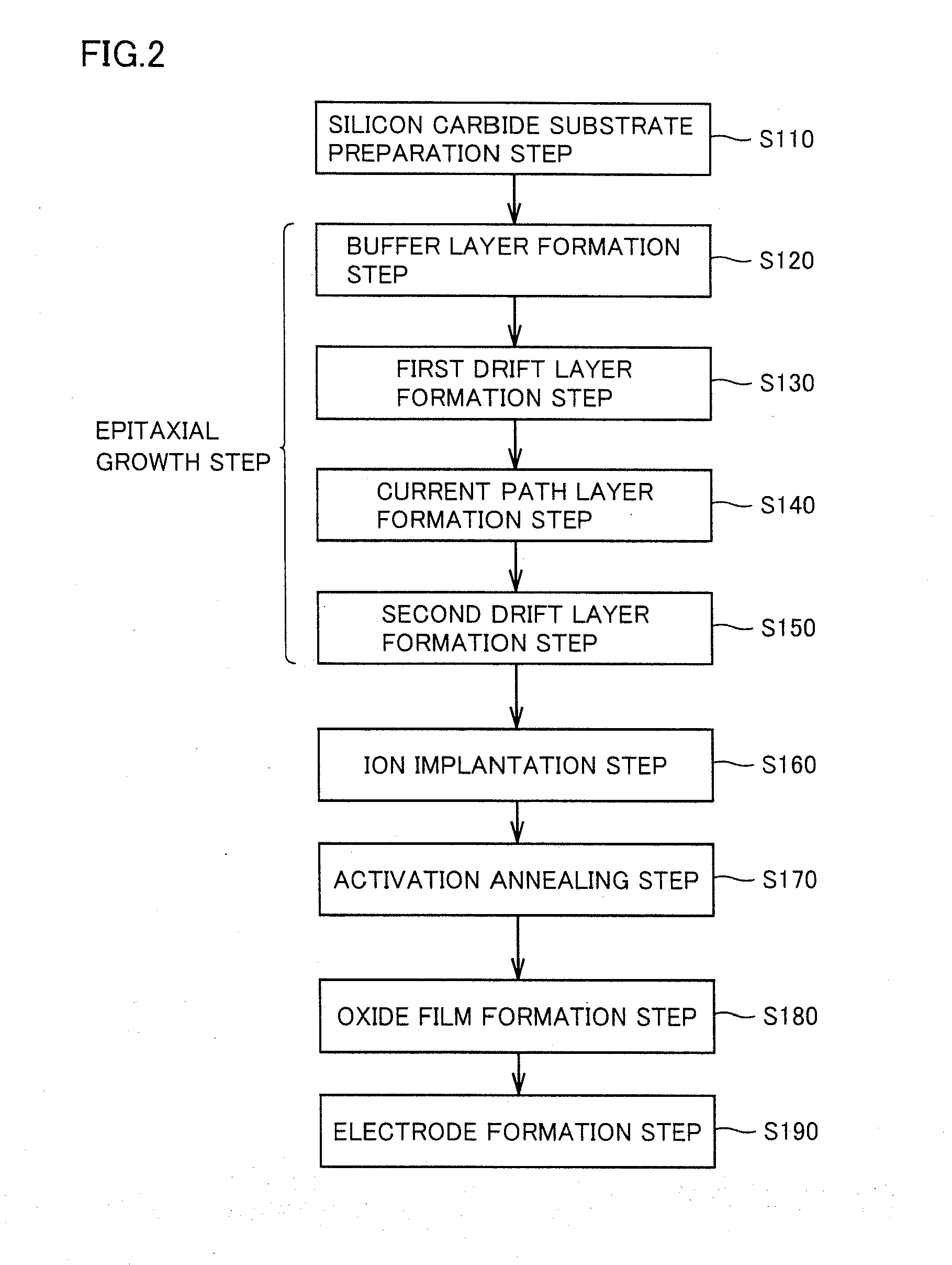
[0020]An embodiment of the present invention will be described hereinafter with reference to the drawings. It is noted that the same or corresponding parts have the same reference numerals allotted in the drawings, and description thereof will not be repeated.

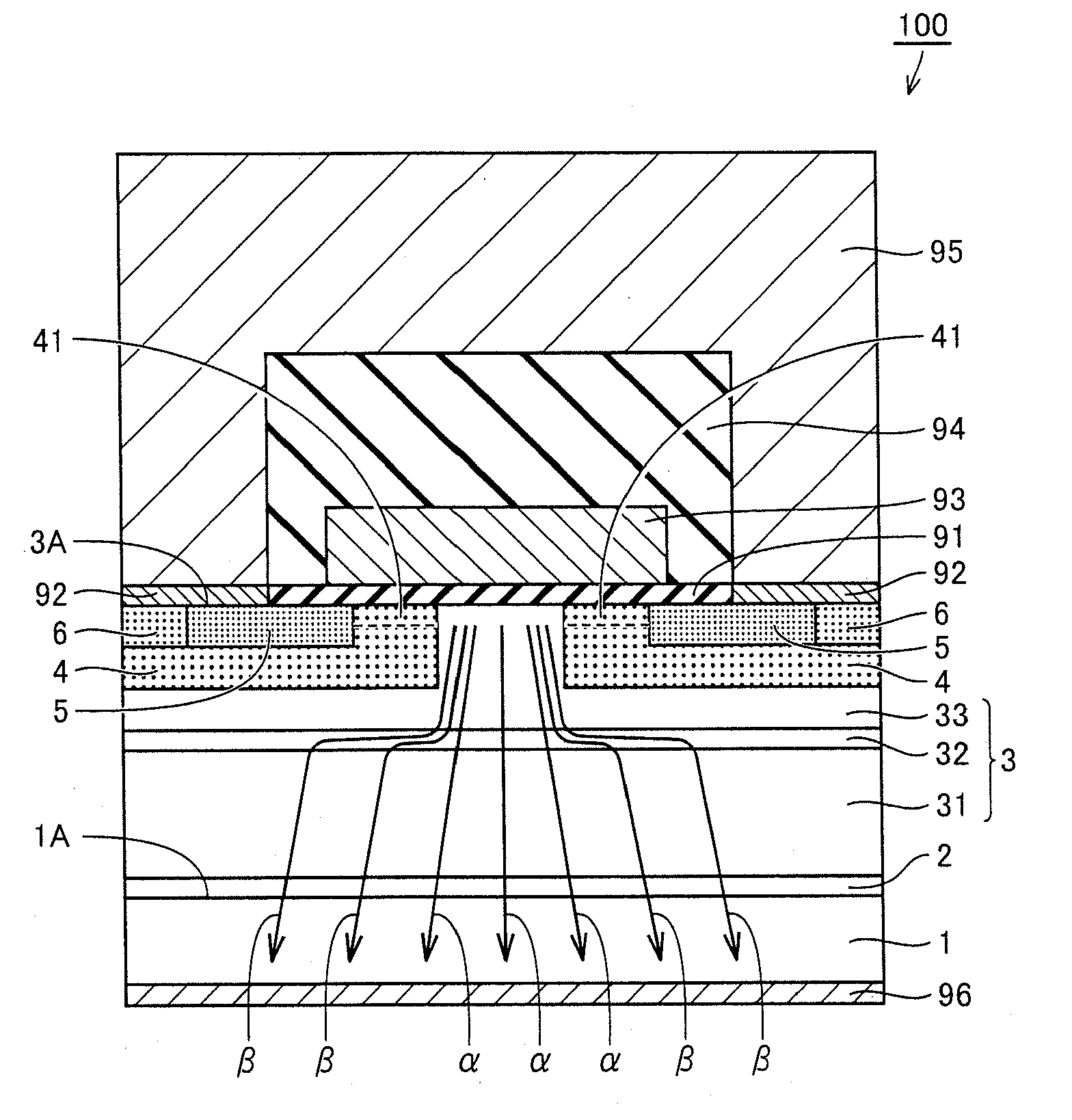
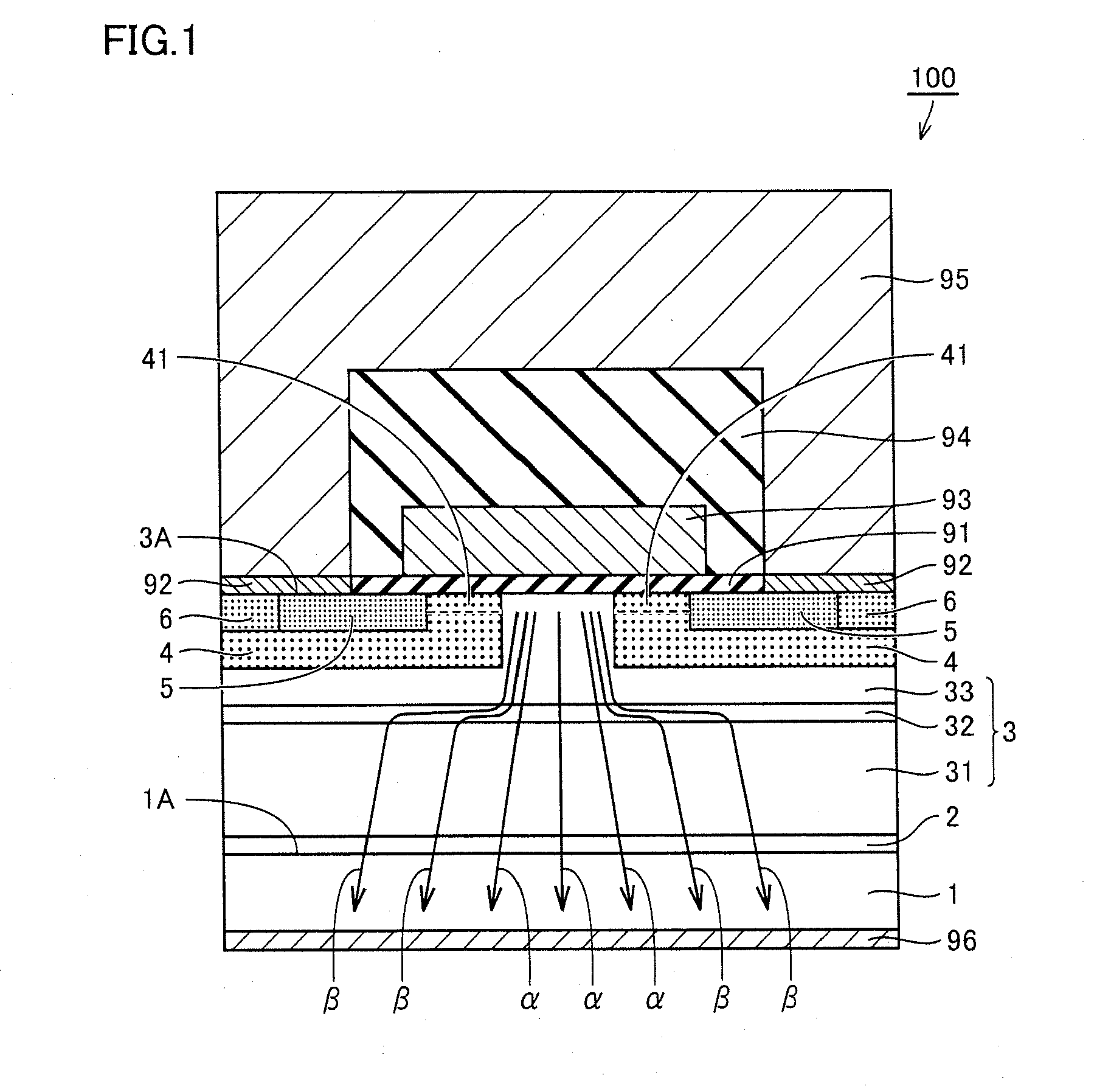
[0021]Referring to FIG. 1, a semiconductor device of one embodiment of the present invention will be described. A MOSFET 100 which is a semiconductor device (DiMOSFET) in this embodiment includes a silicon carbide substrate 1 of an n conductivity type (first conductivity type), a buffer layer 2 of the n conductivity type made of silicon carbide, a drift layer 3 of the n conductivity type made of silicon carbide, a pair of p type body regions 4 of a p conductivity type (second conductivity type), n+ regions 5 of the n conductivity type, and p+ regions 6 of the p conductivity type.

[0022]Buffer layer 2 is formed on one main surface 1A of silicon carbide substrate 1, and is of the n conductivity type by containing an n type impurit...


PUM


Abstract

A MOSFET includes a silicon carbide substrate, a buffer layer made of silicon carbide formed on the silicon carbide substrate, a drift layer made of silicon carbide of an n conductivity type formed on the buffer layer, a p type body region of a p conductivity type formed in the drift layer to include a main surface of the drift layer opposite to the buffer layer, a source contact electrode formed on the p type body region, and a drain electrode formed on a main surface of the silicon carbide substrate opposite to the buffer layer. A current path region having an impurity concentration higher than that of another region in the drift layer is formed in a region in the drift layer sandwiched between the buffer layer and the body region.

Description

BACKGROUND OF THE INVENTION[0001]1. Field of the Invention[0002]The present invention relates to semiconductor devices, and more particularly to a semiconductor device capable of achieving reduction in on-resistance.[0003]2. Description of the Background Art[0004]Semiconductor devices, such as MOSFETs (Metal Oxide Semiconductor Field Effect Transistors) and IGBTs (Insulated Gate Bipolar Transistors), capable of controlling formation of an inversion layer by adjusting a voltage to be applied to a body region to switch between an on state and an off state, have been demanded to achieve increase in breakdown voltage, on-resistance reduction and the like. As power devices demanded to withstand large currents and high voltages, vertical semiconductor devices in which a current flows in the direction of thickness of semiconductor device are used (e.g., see Japanese Patent Laying-Open No. 2009-158788).[0005]With recent demands for higher efficiency and smaller loss, further reduction in on...

Claims


Application Information

Patent Timeline
IPC IPC(8): H01L29/06
CPCH01L29/66068H01L29/7395H01L29/0878H01L21/8213H01L29/7802H01L29/1608
Inventor ITOH, SATOMIMASUDA, TAKEYOSHI
Owner SUMITOMO ELECTRIC IND LTD
Why Eureka
Try Eureka