Semiconductor device and a method for fabricating the device

Inactive Publication Date: 2003-12-18
SEMICON ENERGY LAB CO LTD
View PDF20 Cites 25 Cited by
  • Summary
  • Abstract
  • Description
  • Claims
  • Application Information

AI Technical Summary

Problems solved by technology

The technique can cause a large proportion of crystal grains to orient in the same direction, and can lower the heating temperature required for crystallization as well.
However, the metallic element added for helping crystallization remains in the semiconductor film having a crystal structure, or on the surface thereof, causing problems such as fluctuation in characteristic of semiconductor elements obtained.
In short, the metallic element for helping crystallization becomes an unwanted presence once the semiconductor film having a crystal structure is formed.
In addition to this problem, high concentration phosphorus doping prolongs the treatment time required for doping and lowers the throughput in the do

Method used


Image

  • Semiconductor device and a method for fabricating the device
  • Semiconductor device and a method for fabricating the device
  • Semiconductor device and a method for fabricating the device

Examples


embodiment 1

[0100] Embodiment 1

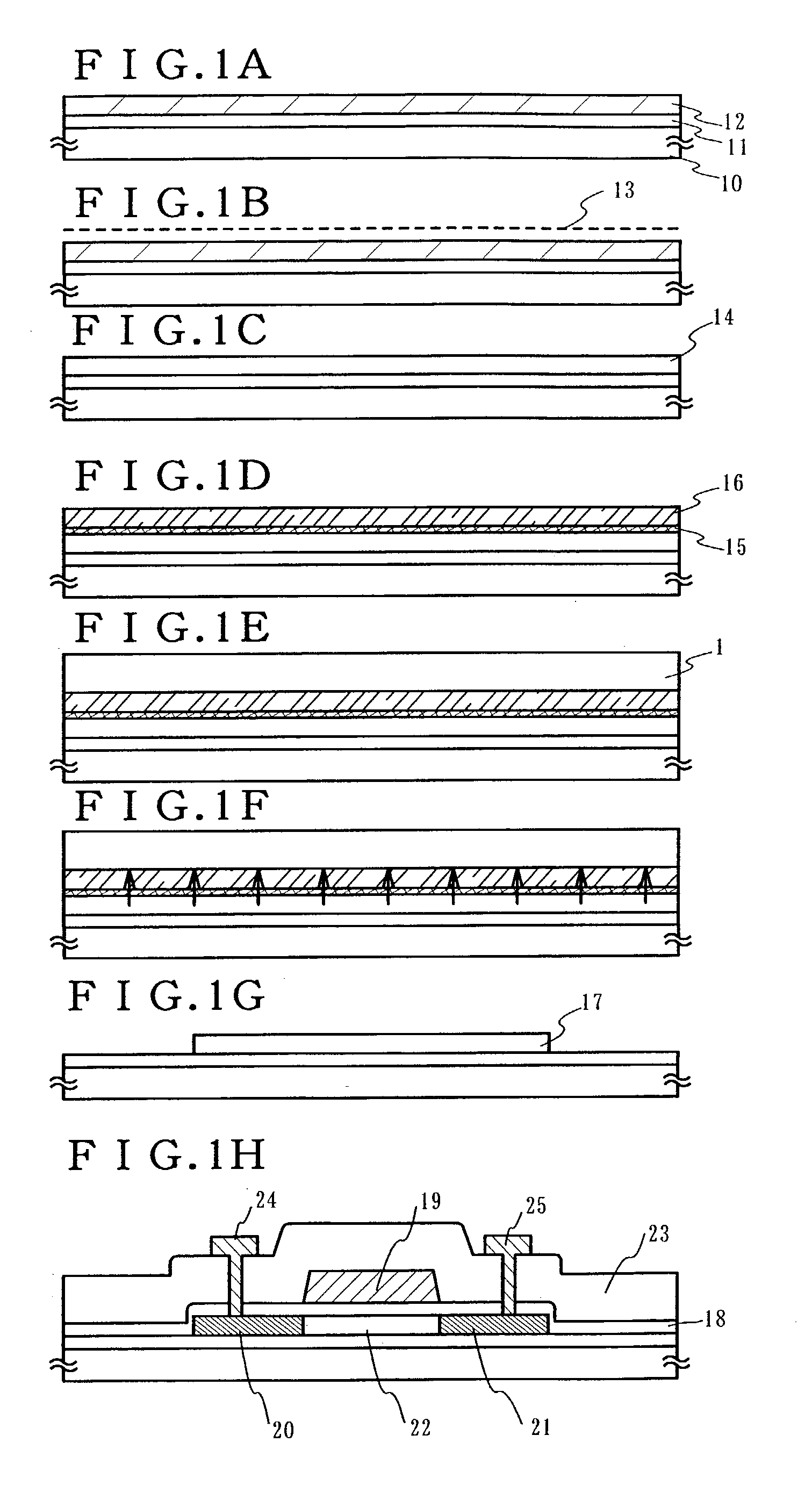
[0101] Embodiments of the present invention will be described with reference to FIGS. 6A to 8. Here, description in detail will be given on a method of fabricating a pixel portion and TFTs (an n-channel TFT and a p-channel TFT) of a driving circuit provided in the periphery of the pixel portion on the same substrate at the same time.

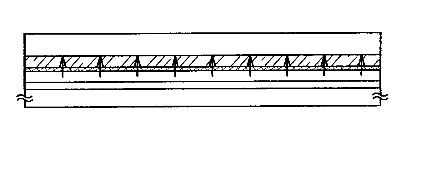
[0102] First, a base insulating film 101 is formed on a substrate 100. After a first semiconductor film having a crystal structure is obtained, the film is etched into desired shapes to form semiconductor layers 102 to 106 that are separated from one another like islands.

[0103] A glass substrate (#1737) is used as the substrate 100, for the base insulating film 101, a silicon oxynitride film 101a with a thickness of 50 nm (preferably 10 to 200 nm) is formed by a plasma CVD method at 400.degree. C. using SiH.sub.4, NH.sub.3, and N.sub.2O as material gas. Next, a silicon oxynitride film 101b with a thickness of 100 nm (preferably 50 to 2...

embodiment 2

[0154] Embodiment 2

[0155] This embodiment describes a process of fabricating an active matrix liquid crystal display device from the active matrix substrate fabricated in Embodiment 1. The description is given with reference to FIG. 9.

[0156] After the active matrix substrate as illustrated in FIG. 8 is obtained in accordance with Embodiment 1, an oriented film is formed on the active matrix substrate of FIG. 8 and subjected to a rubbing treatment. In this embodiment, before the oriented film is formed, an organic resin film such as an acrylic resin film is patterned to form columnar spacers in desired positions in order to keep the substrates apart. The columnar spacers may be replaced by spherical spacers sprayed onto the entire surface of the substrate.

[0157] An opposite substrate is prepared next. The opposite substrate has a color filter in which colored layers and light-shielding layers are arranged with respect to the pixels. A light-shielding layer is also placed in the drivi...

embodiment 3

[0165] Embodiment 3

[0166] Embodiment 1 shows an example of a reflective display device in which a pixel electrode is formed from a reflective metal material. Shown with FIG. 10 in this embodiment is an example of transmissive display device in which a pixel electrode is formed from a light-transmitting conductive film.

[0167] The fabricate processes up through the step of forming an interlayer insulating film are identical with the processes of Embodiment 1, and the description thereof is omitted here. After the interlayer insulating film is formed in accordance with Embodiment 1, a pixel electrode 601 is formed from a light-transmitting conductive film. Examples of the light-transmitting conductive film include an ITO (indium tin oxide alloy) film, an indium oxide-zinc oxide alloy (In.sub.2O.sub.3--ZnO) film, a zinc oxide (ZnO) film, and the like.

[0168] Thereafter, contact holes are formed in an interlayer insulating film 600. A connection electrode 602 overlapping the pixel electro...


PUM


Abstract

A technique, where a semiconductor film having a crystal structure is obtained using a metal element that helps crystallization of the semiconductor film, then that metal element remained in the film is effectively removed, as a result variation among elements is reduced, is provided. In a process for forming a gettering site, a semiconductor film containing a rare-gas element is formed, then an anti-diffusion film for preventing diffusion of the rare-gas element is formed, thereby the metal element in another semiconductor film is effectively removed, particularly in a gettering that is a heating treatment at a high temperature of 600° C. or more.

Description

[0001] 1. Field of the Invention[0002] The present invention relates to a semiconductor device which has circuits structured by thin film transistors (hereafter referred to as TFTs) and to a method for fabricating the same. For example, the present invention relates to an electro-optical device, typically represented by a liquid crystal display panel, and to an electronic apparatus in which a light emitting display device having light emitting elements is installed as a part.[0003] Note that, in the specification, the term, semiconductor devices, indicates a category of general devices which are capable of functioning by utilizing semiconductor characteristics, and electro-optical devices, semiconductor circuits, and electronic apparatuses are all included in the category of semiconductor devices.[0004] 2. Description of the Related Art[0005] Thin film transistors (hereinafter referred to as TFTs) are known as a typical semiconductor element that use a semiconductor film having a cr...

Claims


Application Information

Patent Timeline
IPC IPC(8): H01L21/322H01L21/336H01L21/77H01L21/84H01L27/12H01L29/423H01L29/49H01L29/786
CPCH01L21/3226H01L27/12H01L29/42384H01L27/1277H01L29/66757H01L29/78621H01L29/78675H01L29/4908
Inventor OHNUMA, HIDETO
Owner SEMICON ENERGY LAB CO LTD
Why Eureka
Try Eureka