Semiconductor device and it's manufacturing method

a technology of semiconductors and manufacturing methods, applied in semiconductor devices, transistors, electrical devices, etc., can solve the problems of difficult suppression of junction leakage of drams of a megabit class, difficult to suppress junction leakage at dram portions, and various kinds of problems, so as to achieve sufficient effective channel length, maintain data holding characteristics, and reduce contact resistance

Inactive Publication Date: 2006-08-08
SONY CORP
View PDF12 Cites 25 Cited by
  • Summary
  • Abstract
  • Description
  • Claims
  • Application Information

AI Technical Summary

Benefits of technology

[0018]Accordingly, it becomes possible to secure a withstand voltage across the gate electrode (word line) and the take-out electrode connected to the diffusion layer.
[0019]Further, the gate electrode is provided within the trench formed in the semiconductor substrate through the gate insulating film, and the diffusion layer is formed on the surface side of the semiconductor substrate. Therefore, the channel is formed so as to surround the semiconductor substrate on the bottom side of the trench in which the gate electrode is formed. Accordingly, effective channel length can be sufficiently secured and a back bias voltage may be effectively applied to stabilize the transistor characteristic of the DRAM cell which will suffer from a severe short channel effect. Moreover, it is possible for the take-out electrode to be connected to the diffusion layer on the entire surface on the side of the semiconductor substrate, with a result that the contact resistance can be decreased.
[0020]Furthermore, the word line is formed so as to connect to the gate electrode in the trench which is formed in the semiconductor substrate and the element separating region. Therefore, it is possible to fabricate the word line together with the gate electrode in the same process. Also, the diffusion layer is formed in such a manner that the impurity concentration thereof is decreased as the depth thereof is increased. Thus, it becomes possible to relax the electric field at the junction and the performance of the data holding characteristic can be maintained.

Problems solved by technology

In particular, the manufactures of semiconductor devices intend to develop a complex device having a DRAM with a large capacity and a logic element capable of driving at a high speed fabricated on a single chip.
However, in the piled-type DRAM, various kinds of problems become conspicuous.
As a result, a matter of junction leak at a DRAM portion becomes more and more critical.
Thus, it becomes difficult to suppress the junction leak of DRAM's of a megabit class.
In other words, it becomes difficult to maintain data retention characteristic of DRAM's, which has been easily controlled.
Accordingly, there is no possible solution other than one in which capacitor capacitance is increased for each generation of device.
Furthermore, along with the reduction in size of the DRAM cells, a contact area between a diffusion layer and a take-out electrode also becomes small.
Therefore, scattering of the contact resistance will also influence not only cell transistor but also operation of the DRAM seriously.
If the required film thickness is lowered below this thickness, it is anticipated that employing silicon oxide (SiO2), which has been conventionally employed because of its favorable nature, becomes difficult and that employing new insulating films such as those of zirconium oxide, hafnium oxide, tantalum oxide, aluminum oxide, BST (compound crystal of BaTiO3 and SrTiO3) will become indispensable.
Therefore, the fabrication process of the above replacement gate exhibits an unsatisfactory matching property with a DRAM cell of a stacked type which forms a capacitor with a self aligning contact at an upper portion of the gate electrode.

Method used


Image

  • Semiconductor device and it's manufacturing method
  • Semiconductor device and it's manufacturing method
  • Semiconductor device and it's manufacturing method

Examples


Embodiment Construction

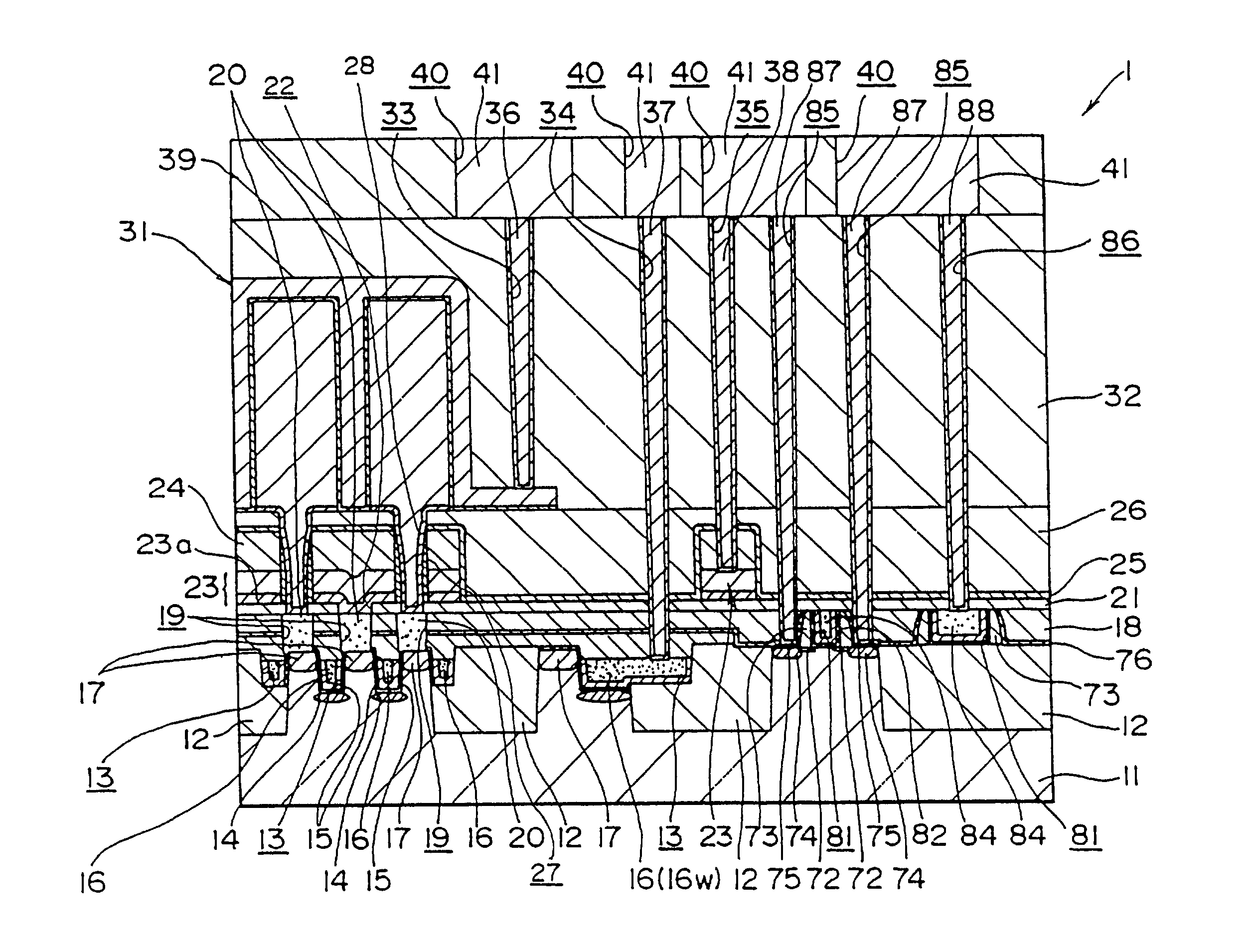
[0029]One example of an embodiment of a semiconductor device according to the present invention will be described with reference to FIG. 1 illustrating a schematic cross-sectional view of a structure of the device.

[0030]As shown in FIG. 1, a semiconductor substrate 11 has an element separating region 12 formed therein.

[0031]The element separating region is formed to have a depth of 0.1 μm to 0.2 μm, for example, by using an STI (Shallow Trench Isolation) technology, for example. A trench 13 is formed in the semiconductor substrate 11 and the element separating region 12 so as to have a depth of approximately 50 nm to 100 nm, for example. In the trench 13, there is provided a word line (gate electrode) 16 through a gate insulting film 15. Even if there is some difference between the depth of the trench 13 formed at the semiconductor substrate 11 and that of the trench 13 formed at the element separating region 12, no problem will be expected.

[0032]A channel diffusion layer 14 is form...


PUM


Abstract

In a semiconductor device having a memory element and a logic element formed on the same semiconductor substrate, a transistor of the memory element comprises a gate electrode (16) embedded within a trench (13) formed in a semiconductor substrate (11) through a gate insulating film (15) and a diffusion layer (17) formed on the side of the semiconductor substrate (11) at a sidewall of the trench (13), and a take-out electrode (20) connected to the diffusion layer (17) is provided so that the take-out electrode overlaps the gate electrode (16) through a first interlayer insulating film (insulating film) (18) on the gate electrode (16). A word line (16) is provided in the trench (13) and an impurity concentration of the diffusion layer (17) is decreased as a depth thereof is increased.

Description

TECHNICAL FIELD[0001]The present invention relates to a semiconductor device and a method of fabricating the device, and more particularly to a semiconductor device in which a DRAM (Dynamic Random Access Memory) and a logic element are fabricated on the device in a mixed fashion and a method of fabricating such a device.BACKGROUND OF THE INVENTION[0002]Manufactures of semiconductor devices are competing every year in rapidly developing microfabrication technology. In particular, the manufactures of semiconductor devices intend to develop a complex device having a DRAM with a large capacity and a logic element capable of driving at a high speed fabricated on a single chip. As an arrangement of one example thereof, memory cell gates of the DRAM are provided on a substrate so that the gates are piled on one another. So-called self aligning contact is introduced to take out a diffusion layer of a memory cell transistor while the logic element is formed without using the self aligning co...

Claims


Application Information

Patent Timeline
Patent Type & Authority Patents(United States)
IPC IPC(8): H01L29/94H01L27/092H01L21/8238H01L21/8242H01L27/108
CPCH01L27/10894H01L27/10876H01L27/10814H01L27/10855H01L27/10891H10B12/315H10B12/0335H10B12/053H10B12/488H10B12/09H10B12/00
Inventor UMEBAYASHI, TAKU
Owner SONY CORP
Why Eureka
Try Eureka