Transistor and method of forming the same

a technology of transistors and transistors, applied in the direction of semiconductor devices, basic electric elements, electrical equipment, etc., can solve the problems of large damage to bulk silicon substrates, reduced channel regions of deltas, etc., and achieve the effect of preventing short channel effect of transistors, high breakdown voltage, and sufficient effective channel length of fin-type transistors

Active Publication Date: 2005-09-08
SAMSUNG ELECTRONICS CO LTD
View PDF6 Cites 28 Cited by
  • Summary
  • Abstract
  • Description
  • Claims
  • Application Information

AI Technical Summary

Benefits of technology

[0025] According to embodiments of the present invention, although a gate structure has a narrow width, an effective channel length of a fin type transistor may be sufficiently ensured. Therefore, a short channel effect of the transistor may be prevented and the fin type transistor may have a high breakdown voltage. Additionally, since the active structure is integrally formed with the substrate and blocking regions are formed under the source / drain regions of the transistor, a junction capacitance of the source / drain regions may be reduced and a leakage current from the source / drain regions may be prevented.

Problems solved by technology

If the protruding portion is spaced apart from the bulk silicon substrate, a channel region of the DELTA may be greatly reduced and also the bulk silicon substrate may be greatly damaged due to a stress generated in the oxidation of the bulk silicon substrate.

Method used


Image

  • Transistor and method of forming the same
  • Transistor and method of forming the same
  • Transistor and method of forming the same

Examples


Embodiment Construction

[0030] The present invention will now be described more fully with reference to the accompanying drawings in which one or more exemplary embodiments of the present invention are shown. In the drawings, the thickness of layers and regions are exaggerated for clarity and like reference numerals refer to like elements throughout. It will be understood that when an element such as an element, layer, region, or substrate is referred to as being “on” or “onto” another element, the element is either directly on the other element or intervening elements may also be present.

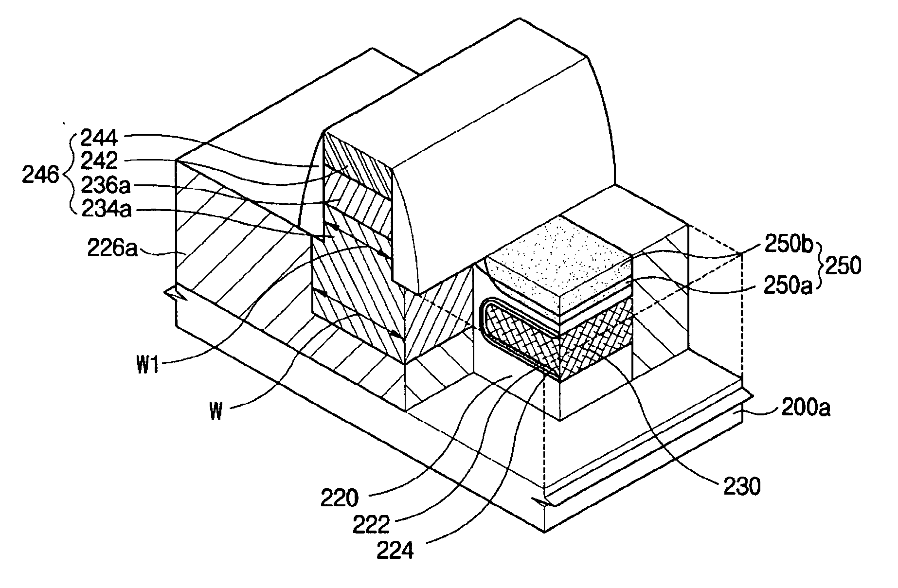
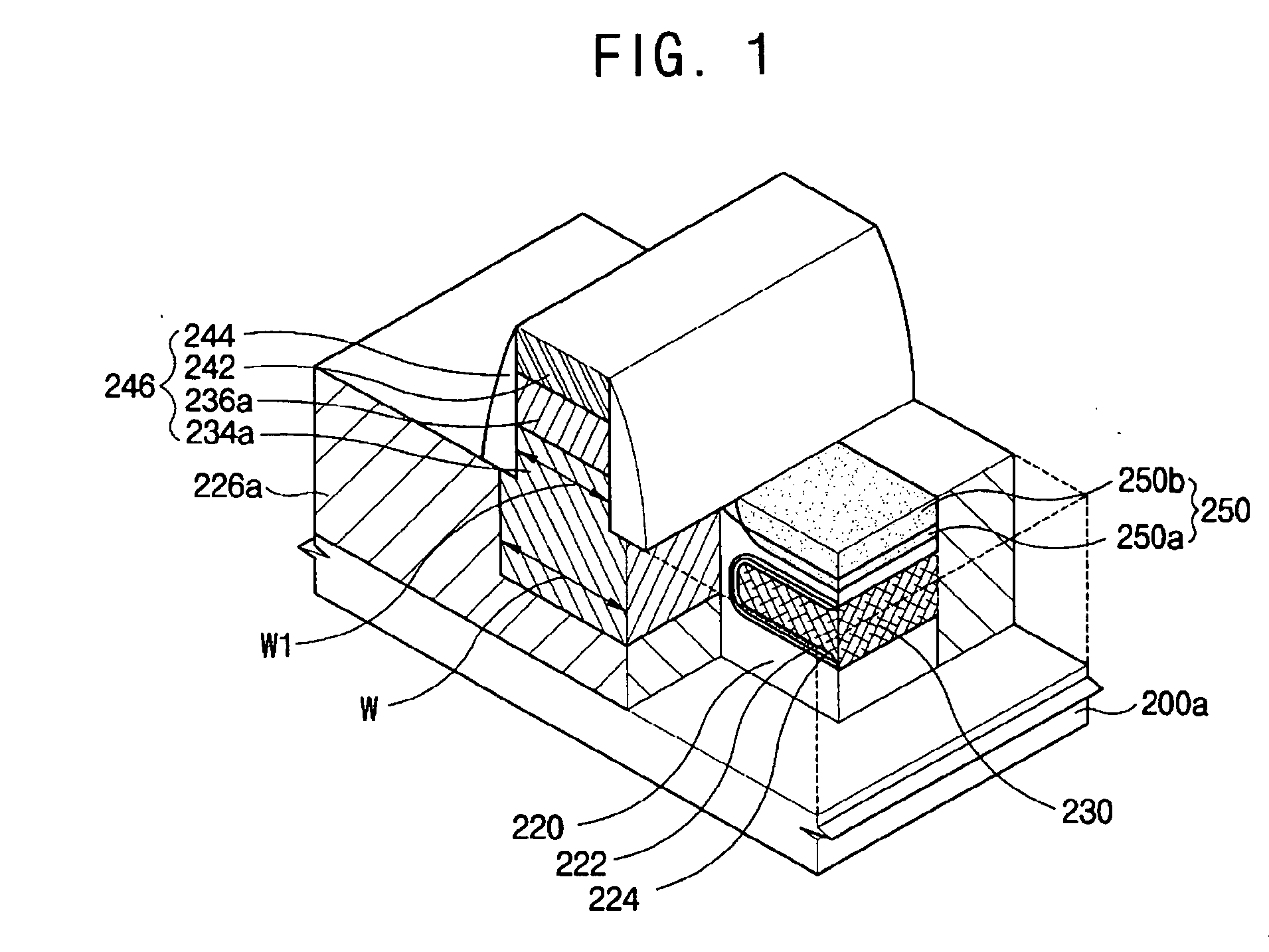
[0031]FIG. 1 is a perspective view of a fin type transistor in accordance with an exemplary embodiment of the present invention.

[0032] Referring to FIG. 1, a fin type transistor of the present invention includes an active structure 220 formed on a semiconductor substrate 200a, an insulation layer pattern 226a, a gate structure 246, source / drain regions 250 and blocking regions 230.

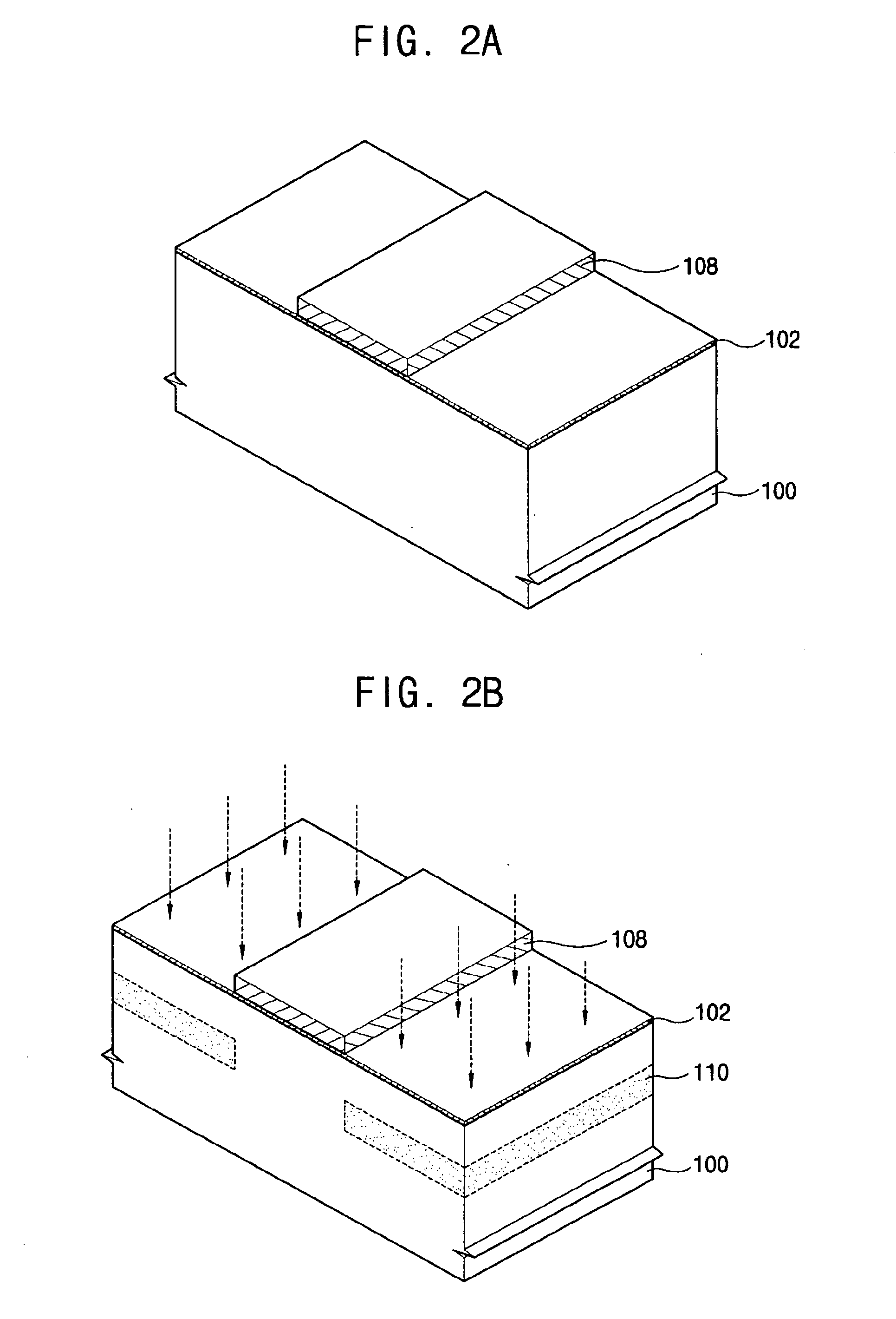
[0033] The semiconductor substrate 200...


PUM


Abstract

According to some embodiments of the invention, a fin type transistor includes an active structure integrally formed with a silicon substrate. The active structure includes grooves that form blocking regions under source/drain regions. A gate structure is formed to cross the upper face of the active structure and to cover the exposed side surfaces of the lateral portions of the active structure. An effective channel length of a fin type transistor may be sufficiently ensured so that a short channel effect of the transistor may be prevented and the fin type transistor may have a high breakdown voltage.

Description

CROSS REFERENCE TO RELATED APPLICATION [0001] This application claims priority from Korean Patent Application No. 2004-14530 filed on Mar. 4, 2004, the contents of which are incorporated herein by reference in their entirety. BACKGROUND OF THE INVENTION [0002] 1. Field of the Invention [0003] The present invention relates to a semiconductor device and a method of forming the same. More particularly, the present invention relates to a fin type transistor capable of preventing a short channel effect, reducing a leakage current, and reducing a junction capacitance in source / drain regions, and a method of forming the transistor. [0004] 2. Description of the Related Art [0005] As the semiconductor industry rapidly develops, the semiconductor devices have minute sizes and improved degree of integration. Since the semiconductor devices have minute sizes, structures of the semiconductor devices also have minute dimensions. For example, the size of an active region of the semiconductor devic...

Claims


Application Information

Patent Timeline
Patent Type & Authority Applications(United States)
IPC IPC(8): H01L29/78H01L21/335H01L29/76
CPCH01L29/785H01L29/66795H01L29/7831H01L29/78618H01L29/78642H10B12/34H01L29/7813
Inventor YOON, JAE-MANLEE, CHOONG-HOPARK, DONG-GUNLEE, CHUL
Owner SAMSUNG ELECTRONICS CO LTD
Why Eureka
Try Eureka