Semiconductor device and method for manufacturing the same

a technology of semiconductors and semiconductors, applied in the direction of semiconductor devices, electrical devices, transistors, etc., can solve the problems of low reliability and achieve the effects of reducing oxygen vacancies, favorable reliability, and reducing the concentration of impurities

Inactive Publication Date: 2017-10-26
SEMICON ENERGY LAB CO LTD
View PDF1 Cites 24 Cited by
  • Summary
  • Abstract
  • Description
  • Claims
  • Application Information

AI Technical Summary

Benefits of technology

[0011]An object of one embodiment of the present invention is to provide a semiconductor device having favorable reliability. Another object of one embodiment of the present invention is to provide a semiconductor device including an oxide semiconductor in which the concentration of impurities is reduced. Another object of one embodiment of the present invention is to provide a semiconductor device including an oxide semiconductor in which oxygen vacancies are reduced.

Problems solved by technology

However, it is known that a transistor including an oxide semiconductor as an active layer has a problem in that the electrical characteristics are easily changed by impurities and oxygen vacancies in the oxide semiconductor and thus the reliability is low.

Method used


Image

  • Semiconductor device and method for manufacturing the same
  • Semiconductor device and method for manufacturing the same
  • Semiconductor device and method for manufacturing the same

Examples


embodiment 1

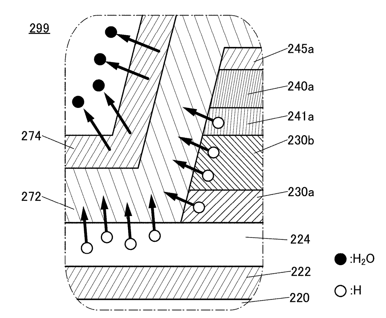
[0079]In this embodiment, a semiconductor device including a transistor having favorable reliability and a method for manufacturing the semiconductor device are described with reference to FIGS. 1A to 1E through FIGS. 27A to 27E. A transistor provided in a semiconductor device of this embodiment includes an oxide semiconductor in an active layer. The reliability of the transistor provided in the semiconductor device can be improved by reducing the concentration of impurities such as water or hydrogen in the oxide semiconductor and reducing oxygen vacancies by supplying excess oxygen.

[0080]1000>

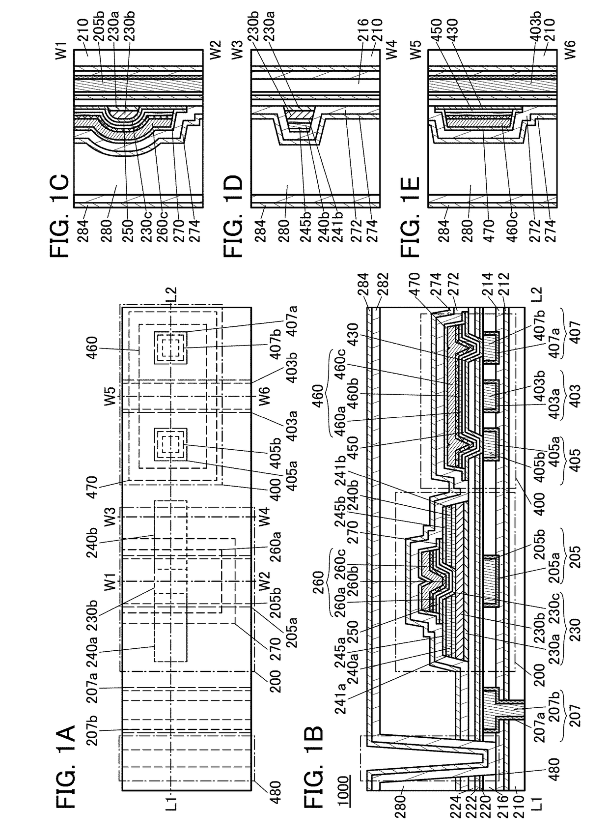
[0081]FIGS. 1A to 1E are a top view and cross-sectional views of a semiconductor device 1000. The semiconductor device 1000 includes a transistor 200 and a transistor 400. The transistors 200 and 400 formed over a substrate (not illustrated) have different structures. For example, the transistor 400 may have a smaller drain current than the transistor 200 when a back gate voltage and a top gat...

modification example

[0345]The structure of the semiconductor device in this embodiment is not limited to the structure in FIGS. 1A to 1E. For example, a structure in FIGS. 27A to 27E may be employed.

[0346]The semiconductor device 1000 in FIGS. 27A to 27E is different from the semiconductor device 1000 in FIGS. 1A to 1E in that the opening 480 is formed in the insulators 216, 220, 222, and 224 and the insulator 272 is in contact with the top surface of the insulator 214. Thus, the transistors 200 and 400 are sealed with the insulators 212, 214, 272, and 274. In this case, even when the insulators 282 and 284 are not provided, entry of impurities such as water or hydrogen from the side surfaces of the insulators 216 and 224 can be prevented.

[0347]Moreover, the semiconductor device 1000 in FIGS. 27A to 27E is different from the semiconductor device 1000 in FIGS. 1A to 1E in that the layer 270, the insulator 250, and the oxide 230c extend beyond the end portions of the conductor 260 and overlap with each o...

embodiment 2

[0350]In this embodiment, embodiments of semiconductor devices are described with reference to FIG. 28, FIG. 29, and FIG. 30.

[Memory Device]

[0351]FIGS. 28 to 30 each illustrate an example of a memory device using the semiconductor device of one embodiment of the present invention.

[0352]The memory devices in FIG. 28 and FIG. 29 each include the transistor 400, a transistor 300, the transistor 200, and a capacitor 100. The transistors 200 and 400 are similar to those described in the Embodiment 1.

[0353]The transistor 200 is a transistor in which a channel is formed in a semiconductor layer including an oxide semiconductor. Since the off-state current of the transistor 200 is small, by using the transistor 200 in a memory device, stored data can be retained for a long time. In other words, such a memory device does not require refresh operation or has an extremely low frequency of the refresh operation, which leads to a sufficient reduction in power consumption of the memory device.

[03...


PUM


Abstract

A highly reliable semiconductor device is provided. The semiconductor device includes a first barrier insulating film; a first gate electrode thereover; a first gate insulating film thereover; an oxide semiconductor film thereover; source and drain electrodes over the oxide semiconductor film; a second gate insulating film over the oxide semiconductor film; a second gate electrode over the second gate insulating film; a second barrier insulating film that covers the oxide semiconductor film, the source and the drain electrodes, and the second gate electrode, and is in contact with side surfaces of the oxide semiconductor film and the source and drain electrodes; and a third barrier insulating film thereover. The first to third barrier insulating films are less likely to transmit hydrogen, water, and oxygen than the first and second gate insulating films. The third barrier insulating film is thinner than the second barrier insulating film. The source and drain electrodes each includes a conductive oxide film in contact with the oxide semiconductor film. The conductive oxide film has more oxygen vacancies than the oxide semiconductor film.

Description

BACKGROUND OF THE INVENTION1. Field of the Invention[0001]One embodiment of the present invention relates to a semiconductor device and a method for manufacturing the semiconductor device.[0002]Note that one embodiment of the present invention is not limited to the above technical field. One embodiment of the invention disclosed in this specification and the like relates to an object, a method, or a manufacturing method. In addition, one embodiment of the present invention relates to a process, a machine, manufacture, or a composition of matter.[0003]In this specification and the like, a semiconductor device generally means a device that can function by utilizing semiconductor characteristics. A display device (e.g., a liquid crystal display device or a light-emitting display device), a projection device, a lighting device, an electro-optical device, a power storage device, a memory device, a semiconductor circuit, an imaging device, an electronic device, and the like may include a ...

Claims


Application Information

Patent Timeline
Patent Type & Authority Applications(United States)
IPC IPC(8): H01L29/786H01L29/66H01L27/12H01L27/105
CPCH01L29/78606H01L29/7869H01L29/78648H01L29/66969H01L27/1255H01L27/1207H01L27/1225H01L27/124H01L27/1052H10B99/00
Inventor YAMAZAKI, SHUNPEIMATSUBAYASHI, DAISUKETOKUMARU, RYOYAMANE, YASUMASAOGINO, KIYOFUMIENDO, TAICHIKIMURA, HAJIME
Owner SEMICON ENERGY LAB CO LTD
Why Eureka
Try Eureka