High-voltage power semiconductor device with body regions of alternating conductivity and decreasing thickness

a technology of alternating conductivity and semiconductor devices, which is applied in the direction of semiconductor devices, transistors, electrical devices, etc., can solve the problems of difficult to increase the withstand voltage, reduce the resistance in the drift region, and reduce the loss, so as to reduce the electric field, reduce the resistance, and the effect of high withstand voltag

Inactive Publication Date: 2008-12-30
THE KANSAI ELECTRIC POWER CO
View PDF14 Cites 22 Cited by
  • Summary
  • Abstract
  • Description
  • Claims
  • Application Information

AI Technical Summary

Benefits of technology

[0012]The purpose of the present invention is to provide a semiconductor device with a high withstand voltage that reduces an electric field in a drai

Problems solved by technology

This drastically can reduce the resistance in the drift region.
As a result, the resistance in the drain region increases, the on-resistance increases when the semiconductor device is turned on for flowing a current, and reducing the loss becomes difficult.
The electric field tends to concentrate at the bottom of the recess 110, and it is difficult to increase the withstand voltage.
However, in that case, the electric field increases in the gate insulation film 105 at the bottom of the recess 110, and it is difficult to increase the withstand voltage.
The S

Method used


Image

  • High-voltage power semiconductor device with body regions of alternating conductivity and decreasing thickness
  • High-voltage power semiconductor device with body regions of alternating conductivity and decreasing thickness
  • High-voltage power semiconductor device with body regions of alternating conductivity and decreasing thickness

Examples


first embodiment

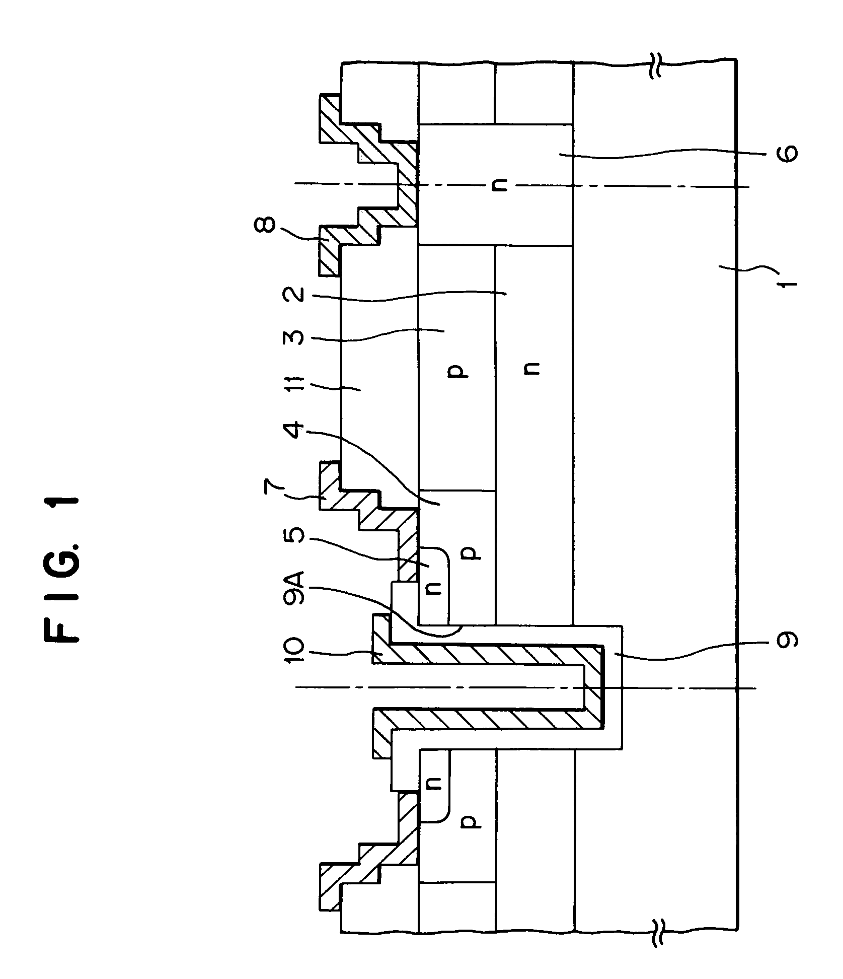
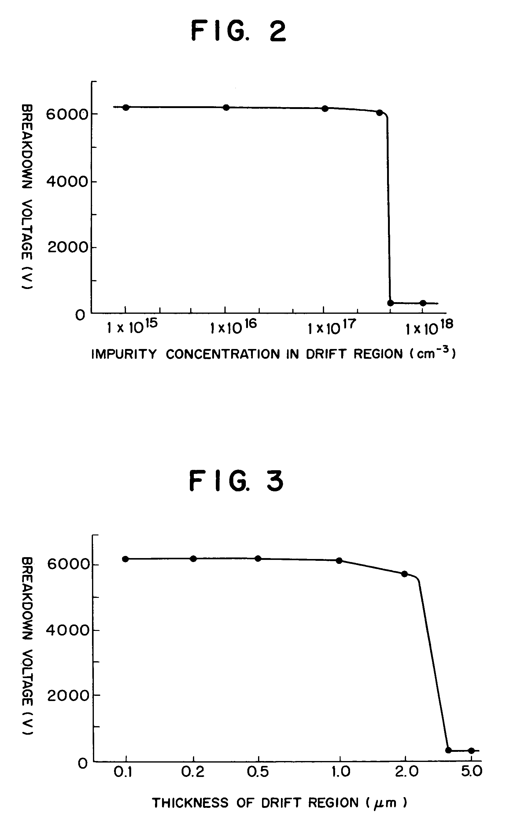
[0058]FIG. 1 is a section view of a semiconductor device of a first embodiment of the present invention. The first embodiment is a wide gap semiconductor device, and is a SiC field effect transistor with a withstand voltage of 6100 V. FIG. 1 shows a sectional structure of segments. A dielectric substrate 1 in the drawing is an extremely high resistance wide gap SiC (silicone carbide) substrate including impurities forming a deep energy level such as vanadium, the resistance ratio is 109 Ωcm or more, and the thickness (a vertical dimension in the drawing) is about 350 μm. A semiconductor device using a SiC substrate is generally referred to a wide gap semiconductor. A first conductive type n-type drift region 2, and a second conductive type p-type drift region 3 formed thereon have approximately the same thickness (virtually the similar thickness), and the same impurity concentration, the thickness is about 0.8 μm and the impurity concentration is about 8×10¹⁶ atm / cm3. With the const...

second embodiment

[0065]FIG. 4 is a section view for showing segments of a SiC field effect transistor of a second embodiment of the present invention. The second embodiment is the same as the first embodiment except for the following three points.

[0066](1) A p-type drift region 12 thinner than the drift region 3 is provided between the drift region 2 and the dielectric substrate 1.

[0067](2) The n-type drain region 6 is formed along the inner wall of a trench 6A reaching to the dielectric substrate 1, the drain region 6 connects with the drift regions 2, 3, and 12, and the drain electrode 8 is provided on the surface of the drain region 6.

[0068](3) The trench 9A is formed so deep as to reach the drift region 12 for the gate electrode 10, and the oxide film 9 and the gate electrode 10 are formed along the inner wall of this trench.

[0069]The thickness of the n-type drift region 2 is 1.3 μm, the thickness of the p-type drift regions 3 and 12 is 0.8 μm, and individual impurity concentrations are about 7×...

third embodiment

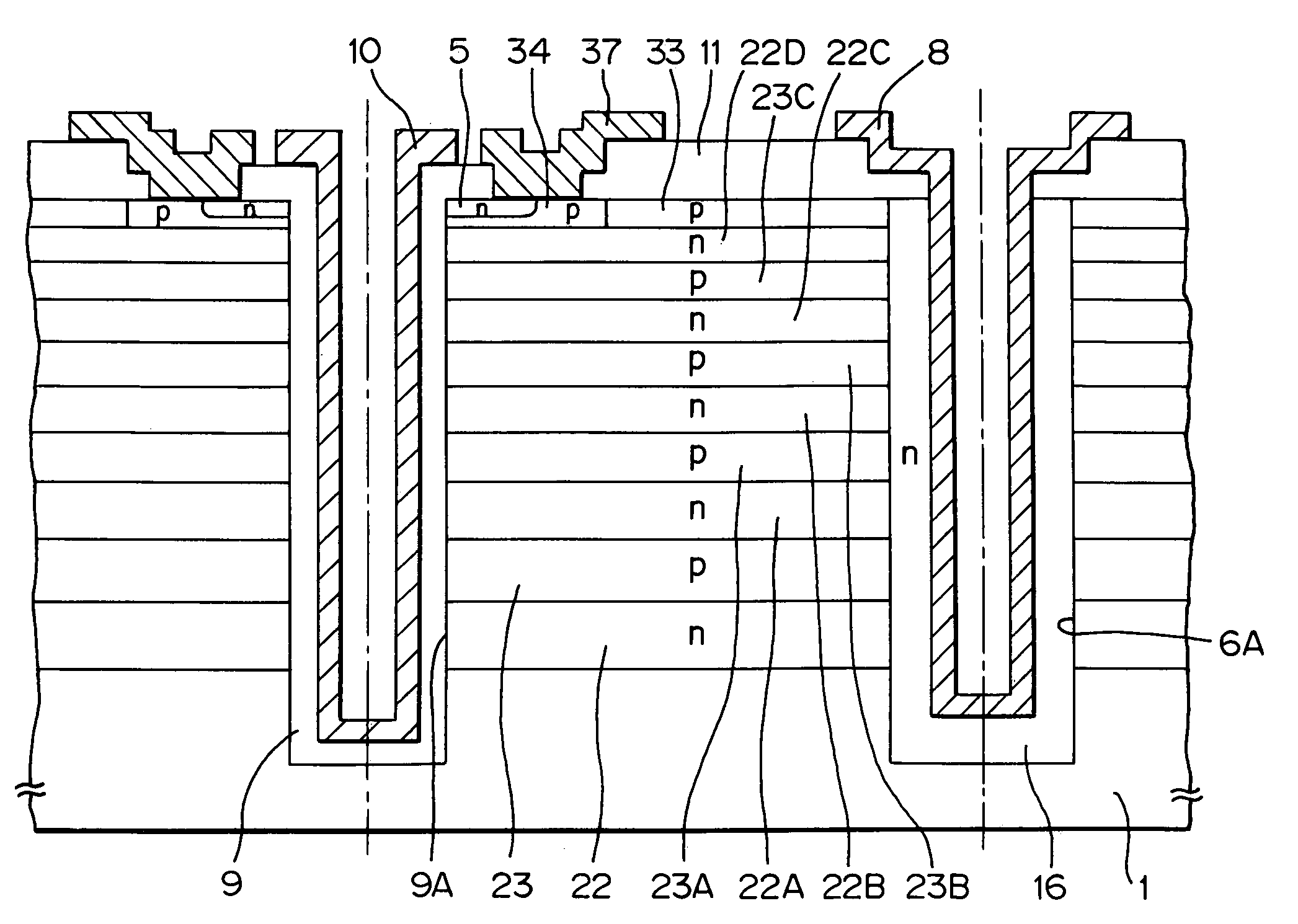
[0073]FIG. 5 is a segment section view of a SiC field effect transistor of a third embodiment of the present invention. Five pairs of an n-type drift region and a p-type drift region are sequentially laminated such that p-type drift regions 23, 23A, 23B, and 23C are respectively laminated between n-type drift regions 22, 22A, 22B, and 22C on the SiC dielectric substrate 1 with the thickness of 320 μm. The trenches 6A and 9A are provided so as to reach the dielectric substrate 1 on both ends of the laminated individual drift regions 22 and 23. The trench 9A is for a gate part, and the gate electrode 10 is provided through the gate oxide film 9. The trench 6A is for a drain part, and a drain region 16 and the drain electrode 8 are provided on the inner wall. A p-type body region 34, the n-type source region 5, and a source electrode 37 connected with these regions are provided on the gate part side of the upper most layer of a p-type drift region 33. The surface protection film 11 suc...


PUM


Abstract

A semiconductor device which eases an electric field at a drift portion without a reduction in impurity concentrations, and has a high withstand voltage and a low on-resistance, wherein, when a rated voltage is applied between a body region and a drain region formed on an insulating semiconductor substrate, the thicknesses of two, p-type and n-type, drift regions sandwiched between the body and drain regions are selected so as to completely deplete the drift regions.

Description

FIELD OF THE INVENTION[0001]The present invention relates to a semiconductor device, and specifically relates to a power semiconductor device having a high withstand voltage.BACKGROUND ART[0002]Because a wide-gap semiconductor material typified by silicon carbide (abbreviated as SiC hereinafter) has higher dielectric breakdown electric field strength than that of a silicon (abbreviated as Si hereinafter) semiconductor material, it can realize a higher withstand voltage with the same impurity concentration as Si. Further, because SiC has a high withstand voltage while maintaining a low loss, operates at a high temperature of 250° C. or more, has an advantage of an excellent thermal conduction, it is expected as a material for a next generation power semiconductor.[0003]In the “Proceedings of the 10th International Symposium on Power Semiconductor Devices & ICs” published in 1998 it is described a power MOS FET using SiC, and having a structure shown in FIG. 15 in pages 119 to 122. Th...

Claims


Application Information

Patent Timeline
IPC IPC(8): H01L29/08H01L29/06H01L29/10H01L29/16H01L29/20H01L29/22H01L29/24H01L29/267H01L29/417H01L29/423H01L29/739H01L29/74H01L29/744H01L29/749H01L29/78
CPCH01L29/0634H01L29/7393H01L29/7394H01L29/7436H01L29/744H01L29/749H01L29/7816H01L29/7825H01L29/1095H01L29/1602H01L29/1608H01L29/2003H01L29/22H01L29/267H01L29/41716H01L29/41725H01L29/41766H01L29/42368H01L29/7809
Inventor SUGAWARA, YOSHITAKA
Owner THE KANSAI ELECTRIC POWER CO
Why Eureka
Try Eureka