
Array substrate, manufacturing method thereof, and display device

A technology of an array substrate and a manufacturing method, which is applied in the display field, can solve the problems of abnormal loudness electrode signals, affecting the display effect, and the interference of data lines to pixel electrodes, so as to reduce the interference, improve the display effect, and reduce the interlayer capacitance.

Active Publication Date: 2016-05-25
BEIJING BOE OPTOELECTRONCIS TECH CO LTD
View PDF5 Cites 0 Cited by
  • Summary
  • Abstract
  • Description
  • Claims
  • Application Information

AI Technical Summary

Problems solved by technology

In this way, the interference of the data line on the pixel electrode is relatively serious, and the signal of the loudness electrode will be abnormal, which will affect the display effect.

Method used


Image

  • Array substrate, manufacturing method thereof, and display device
  • Array substrate, manufacturing method thereof, and display device
  • Array substrate, manufacturing method thereof, and display device

Examples


Embodiment Construction

[0057] The following will clearly and completely describe the technical solutions in the embodiments of the present invention with reference to the accompanying drawings in the embodiments of the present invention. Obviously, the described embodiments are only some, not all, embodiments of the present invention.

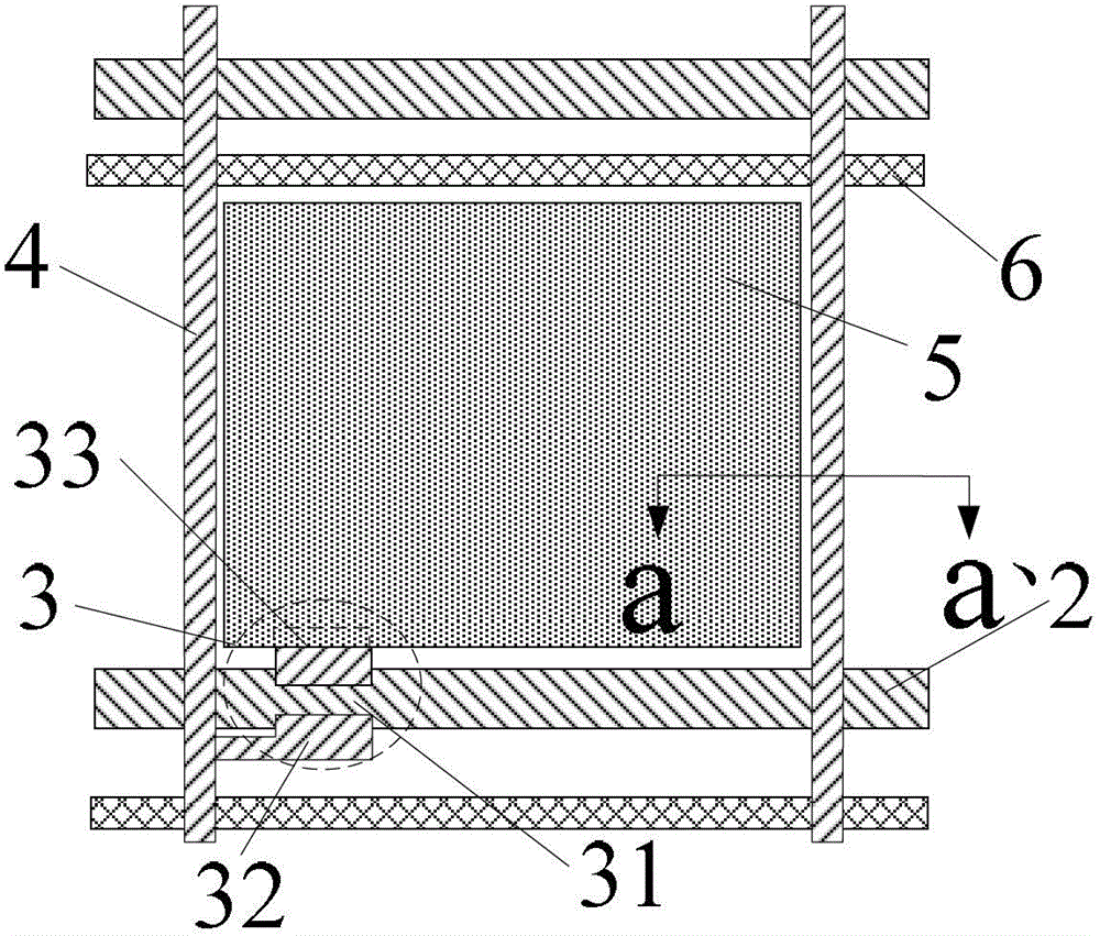
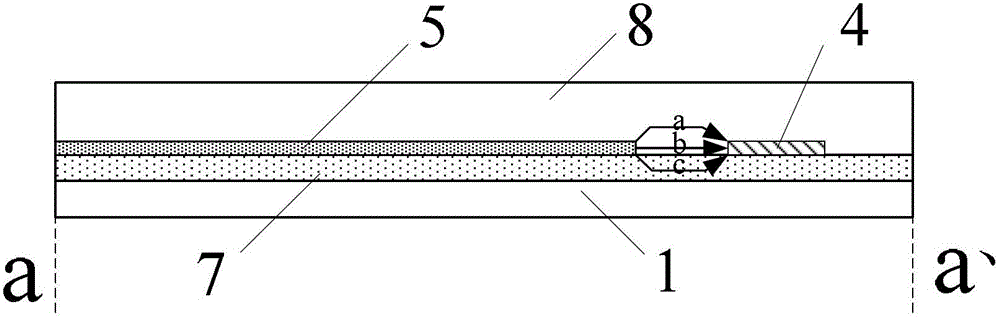
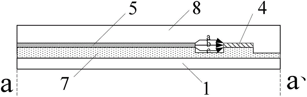
[0058] An embodiment of the present invention provides an array substrate, such as Figure 3-Figure 9 As shown, it includes a gate insulating layer 7, a pixel electrode layer 8, and a data line metal layer arranged on a base substrate, wherein the data line metal layer includes a data line 4, and the pixel electrode layer includes a pixel electrode 5; the gate insulating layer 7 corresponds to The thickness of the region between the pixel electrode 5 and the data line 4 is smaller than the thickness of the region of the gate insulating layer 7 corresponding to the pixel electrode 5 and / or the thickness of the region of the gate insulating layer 7 corresponding to the ...


PUM


Abstract

An array substrate, a manufacturing method therefor, and a display apparatus. The array substrate comprises a gate insulation layer (7), a pixel electrode layer and a data line metal layer all disposed on a base substrate (1). The data line metal layer comprises a data line (4). The pixel electrode layer comprises a pixel electrode (5). The thickness of an area corresponding to an area between the pixel electrode (5) and the data line (4), of the gate insulation layer (7) is smaller than the thickness of an area corresponding to the pixel electrode (5), of the gate insulation layer (7) and / or the thickness of an area corresponding to data line (4), of the gate insulation layer (7).

Description

technical field [0001] The present invention relates to the field of display technology, in particular to an array substrate, a manufacturing method thereof, and a display device. Background technique [0002] An existing liquid crystal display panel includes an array substrate, a color filter substrate, and liquid crystals arranged between the array substrate and the color filter substrate. Such as figure 1 , figure 2 As shown, the array substrate in the liquid crystal display includes: a transparent substrate 1 and a gate metal layer, a gate insulating layer 7, an active layer 8, a source-drain metal layer and a transparent conductive layer arranged on the transparent substrate 1 in sequence, wherein the gate metal The layers include: gate lines 2 and gates 31 , the source-drain metal layer includes: data lines 4 , common electrode lines 6 , source electrodes 32 and drain electrodes 33 , and the transparent conductive layer includes: pixel electrodes 5 . Such as figu...

Claims


Application Information

Patent Timeline
Patent Type & Authority Patents(China)
IPC IPC(8): H01L27/12H01L29/786H01L21/77
CPCG02F1/133345G02F1/136286G02F2202/42G02F1/133357H01L27/124H01L27/1248
Inventor 郭建
Owner BEIJING BOE OPTOELECTRONCIS TECH CO LTD
Learn More