Liquid crystal display panel and manufacturing method of TFT (Thin Film Transistor) array substrate of liquid crystal display panel

A liquid crystal display panel and array substrate technology, which is applied in semiconductor/solid-state device manufacturing, optics, instruments, etc., can solve the problems of reducing the aperture ratio of the display panel, so as to ensure the aperture ratio, increase the transmittance, and eliminate the formation of black streaks Effect

Inactive Publication Date: 2013-12-04
NANJING CEC PANDA LCD TECH
View PDF2 Cites 8 Cited by
  • Summary
  • Abstract
  • Description
  • Claims
  • Application Information

AI Technical Summary

Problems solved by technology

[0006] Purpose of the invention: to solve the problem of the existing photo-alignment VA-type liquid crystal display

Method used


Image

  • Liquid crystal display panel and manufacturing method of TFT (Thin Film Transistor) array substrate of liquid crystal display panel
  • Liquid crystal display panel and manufacturing method of TFT (Thin Film Transistor) array substrate of liquid crystal display panel
  • Liquid crystal display panel and manufacturing method of TFT (Thin Film Transistor) array substrate of liquid crystal display panel

Examples


Embodiment Construction

[0028] Below in conjunction with accompanying drawing and specific embodiment, further illustrate the present invention, it should be understood that these embodiments are only used to illustrate the present invention and are not intended to limit the scope of the present invention, after having read the present invention, those skilled in the art understand various aspects of the present invention Modifications in equivalent forms all fall within the scope defined by the appended claims of this application.

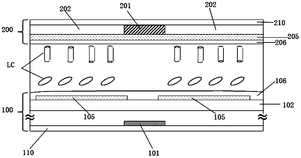
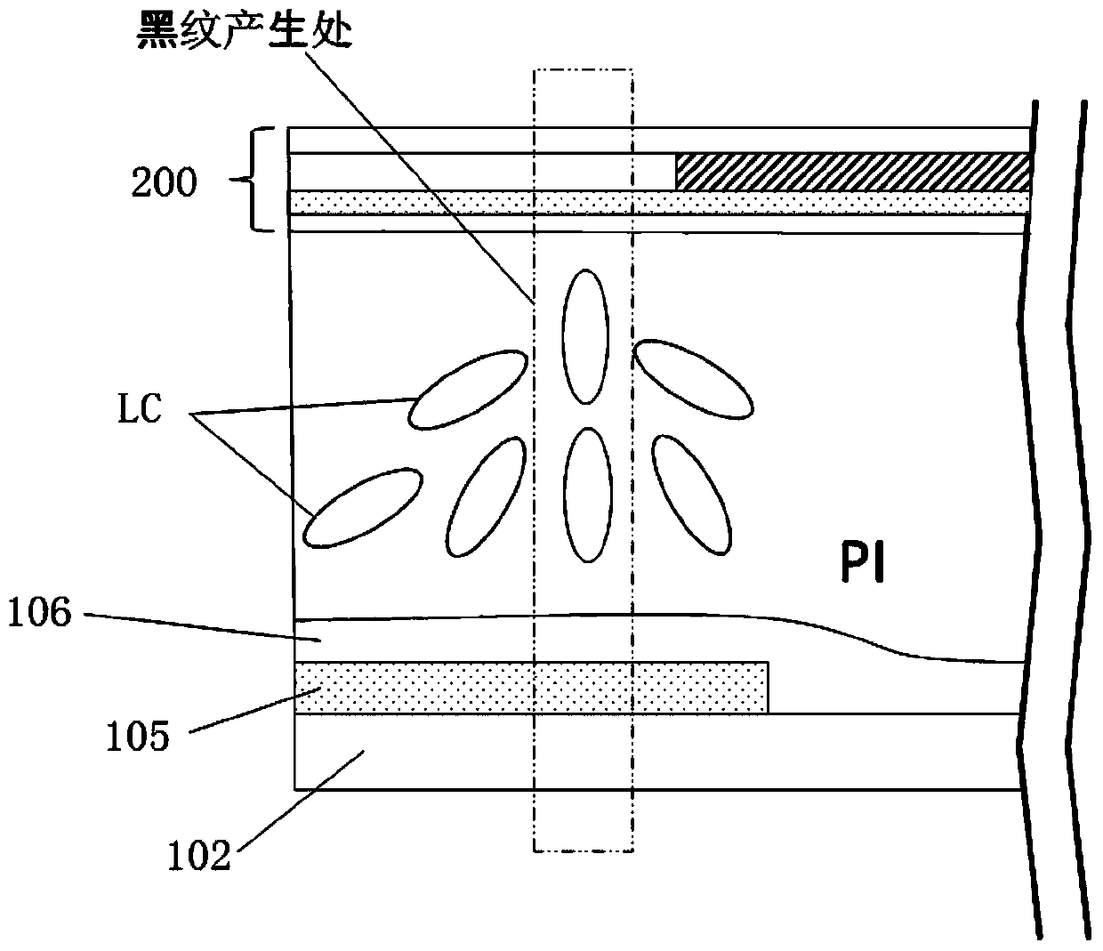
[0029] refer to Figure 4 , which is a cross-sectional view of a liquid crystal display panel according to the first embodiment of the present invention. A liquid crystal display panel provided by the invention improves the flat layer of the existing liquid crystal display panel. like image 3 As shown, the liquid crystal display panel includes a color filter substrate 200 , a TFT array substrate 300 opposite to the color filter substrate 200 , and a plurality of liqui...


PUM

PropertyMeasurementUnit
Thicknessaaaaaaaaaa
Widthaaaaaaaaaa
Depthaaaaaaaaaa

Abstract

The invention discloses a liquid crystal display panel. The liquid crystal display comprises a color film substrate, a TFT (Thin Film Transistor) array substrate arranged opposite to the color film substrate, a liquid crystal positioned between the color film substrate and the TFT array substrate and a flat layer, wherein the TFT array substrate comprises a plurality of pixel regions crossed and limited by a plurality of scanning lines and a plurality of data lines; a plurality of pixel electrodes and a plurality of TFTs which are positioned in the pixel regions; the TFTs are electrically connected with the corresponding pixel electrodes, and the TFTs are further electrically connected with the corresponding scanning lines and data lines; the flat layer is formed on the TFTs and the data lines and covers the TFTs and the data lines; and the flat layer is provided with a plurality of grooves; and the pixel electrodes are positioned above the flat layer and extend to the groove area. Through the technical scheme, when VA (Vertical Arrangement) liquid crystal molecules are driven, the VA liquid crystal molecules above the pixel electrodes can be inclined towards the edge direction correctly, and a region with black lines is limited outside the pixel regions, so that the opening rate when the pixel electrodes are driven can be ensured, and the transmissivity of VA liquid crystal display is effectively improved.

Description

technical field [0001] The invention relates to a manufacturing method of a liquid crystal display panel and its TFT array substrate, in particular to a manufacturing method of a vertical alignment liquid crystal display panel and its TFT array substrate. Background technique [0002] Optically aligned VA (Vertical Alignment, Vertical Alignment) liquid crystal display panels are widely favored by manufacturers for their advantages of simple panel structure, simple manufacturing process, and high aperture ratio. [0003] like figure 1 Shown is a cross-sectional view of a VA-type liquid crystal display panel, which includes a TFT array substrate 100, a color filter substrate 200, and a plurality of liquid crystal molecules LC located between the TFT array substrate and the color filter substrate. Wherein, the color filter substrate 200 includes a color filter glass substrate 210, a black matrix 201 and an RGB color resistance 202 disposed on the glass substrate 210, a conduct...

Claims


Application Information

Patent Timeline
IPC IPC(8): G02F1/1362G02F1/1368G02F1/139H01L21/84
Inventor 洪孟逸
Owner NANJING CEC PANDA LCD TECH
Why Eureka
Try Eureka