Check patentability & draft patents in minutes with Patsnap Eureka AI!

System and method for signal amplification with a dual-gate bio-field effect transistor

A technology of gate structure and source, applied in semiconductor devices, semiconductor/solid-state device manufacturing, measurement devices, etc.

Active Publication Date: 2013-12-04
TAIWAN SEMICON MFG CO LTD
View PDF4 Cites 11 Cited by
  • Summary
  • Abstract
  • Description
  • Claims
  • Application Information

AI Technical Summary

Problems solved by technology

Although BioFET is advantageous in many respects, for example, due to compatibility issues between semiconductor manufacturing processes, biological applications, constraints and/or limitations on semiconductor manufacturing p

Method used


Image

  • System and method for signal amplification with a dual-gate bio-field effect transistor
  • System and method for signal amplification with a dual-gate bio-field effect transistor
  • System and method for signal amplification with a dual-gate bio-field effect transistor

Examples


Embodiment Construction

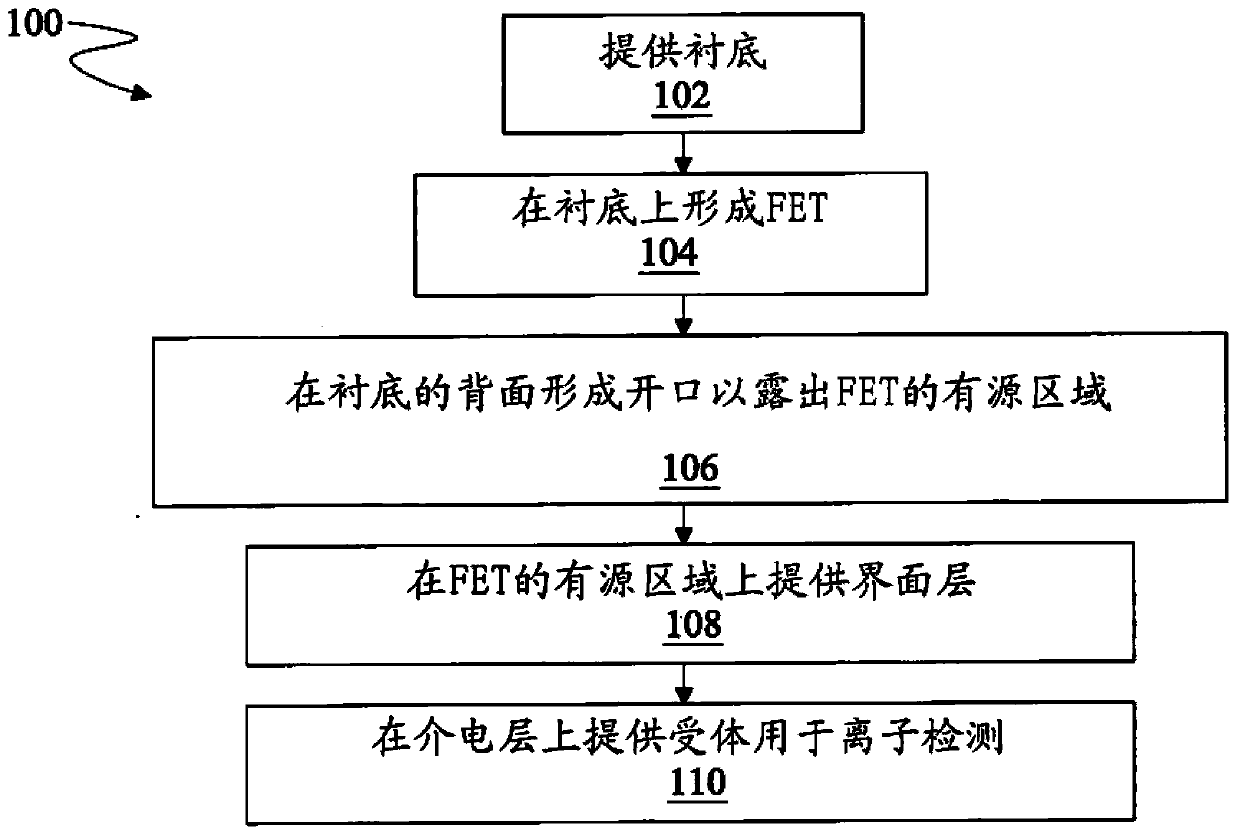
[0039] It is understood that the following disclosure provides many different embodiments, or examples, for implementing various elements of the invention. Specific examples of components and arrangements are described below to simplify the present disclosure. These are of course merely examples and are not intended to be limiting. Also, the formation of the first component over or on the second component in the following description may include an embodiment in which the first component and the second component are formed in direct contact, and may also include an embodiment in which it may be formed between An additional component between the first component and the second component such that the first component and the second component may not be in direct contact. Furthermore, references to relative terms such as "top," "front," "bottom" and "back" are used to provide relative relationships between elements and are not intended to denote any absolute orientation. Various...


PUM


Abstract

The present disclosure provides a bio-field effect transistor (BioFET) and a method of fabricating a BioFET device. The method includes forming a BioFET using one or more process steps compatible with or typical to a complementary metal-oxide-semiconductor (CMOS) process. The BioFET device may include a substrate; a gate structure disposed on a first surface of the substrate and an interface layer formed on the second surface of the substrate. The interface layer may allow for a receptor to be placed on the interface layer to detect the presence of a biomolecule or bio-entity. An amplification factor of the BioFET device may be provided by a difference in capacitances associated with the gate structure on the first surface and with the interface layer formed on the second surface. The invention further provides a system and a method for signal amplification with a dual-gate bio-field effect transistor.

Description

[0001] priority information [0002] This application claims priority to nonprovisional patent application 13 / 480,161, filed May 24, 2012, entitled "CMOS COMPATIBLE BIOFET," which claims nonprovisional patent application 13 / 480,161, filed October 31, 2011, entitled " CMOS COMPATIBLE BIOFET" is the priority of provisional application Serial No. 61 / 553,606. The entire contents of these applications are hereby incorporated by reference. technical field [0003] The present invention relates to the field of semiconductors, and more particularly, the present invention relates to a system and method for signal amplification with double-gate biofield effect transistors. Background technique [0004] Biosensors are devices for sensing and detecting biomolecules and operate on the basis of electronic, electrochemical, optical and mechanical detection principles. Biosensors comprising transistors are sensors that electrically sense charge, photons and mechanical properties of biolog...

Claims


Application Information

Patent Timeline
IPC IPC(8): H01L29/78H01L29/49H01L21/336G01N27/414
CPCG01N27/4145
Inventor 刘怡劭拉希德·巴希尔赖飞龙郑钧文
Owner TAIWAN SEMICON MFG CO LTD
Features
  • R&D
  • Intellectual Property
  • Life Sciences
  • Materials
  • Tech Scout
  • Unparalleled Data Quality
  • Higher Quality Content
  • 60% Fewer Hallucinations
Learn More