
Elastic probe array multi-channel resistance measurement method and device

An elastic probe and resistance measurement technology, applied in the direction of measuring devices, measuring electrical variables, measuring resistance/reactance/impedance, etc., can solve problems such as not saving time, achieve fast non-destructive measurement, shorten measurement time, and improve spatial resolution Effect

Inactive Publication Date: 2013-12-25
INST OF PHYSICS - CHINESE ACAD OF SCI
View PDF6 Cites 7 Cited by
  • Summary
  • Abstract
  • Description
  • Claims
  • Application Information

AI Technical Summary

Problems solved by technology

But the measurement itself doesn't save a lot of time

Method used


Image

  • Elastic probe array multi-channel resistance measurement method and device
  • Elastic probe array multi-channel resistance measurement method and device

Examples


Embodiment Construction

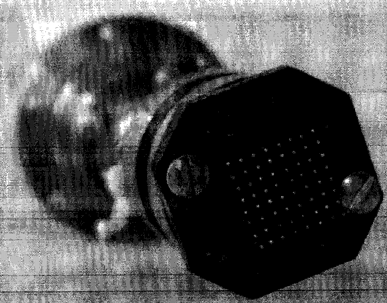
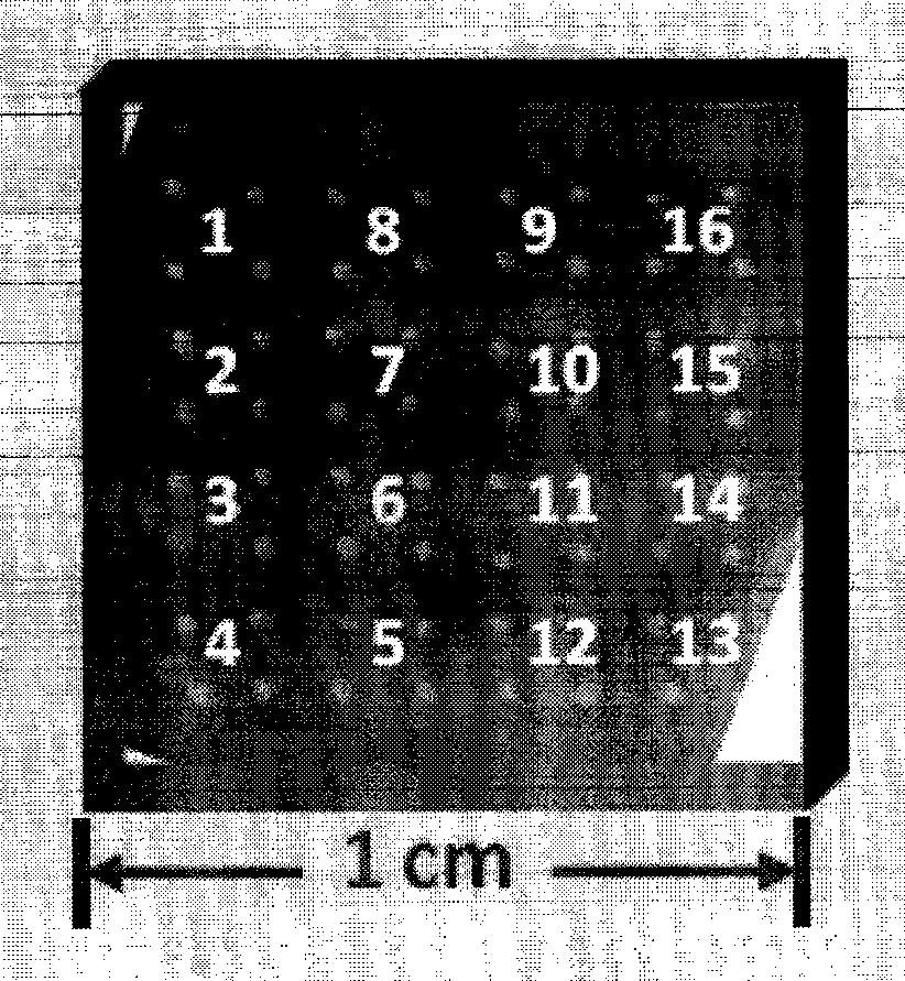
[0016] will be measured as figure 1 The elastic probe assembly shown in , is pressed directly against the sample and placed into a temperature or magnetic field measurement platform. The elastic probe device has a square measurement area of ​​1 cm × 1 cm, the above-mentioned measurement area includes an elastic probe array, and the elastic probe array is an n × n microspring probe array, where n=4 × k, k is greater than An integer equal to 2.

[0017] figure 1 The elastic probe arrays shown in include but are not limited to 8×8 microspring probe arrays, that is, 64 probes are integrated in the above-mentioned 1cm×1cm square measurement area, and between every two nearest neighbor measurement points The spacing is less than 1mm.

[0018] Corresponding to the above-mentioned elastic probe device, for example, the binary composite film prepared by the co-magnetron sputtering method is cut into small pieces of 1 cm×1 cm, and the distance between every two nearest neighbor measu...


PUM


Abstract

The invention provides an elastic probe array multi-channel resistance measurement method compatible with a temperature or magnetic field platform and a probe device. The measurement method comprises the steps that during measurement, an elastic probe array is directly and tightly pressed on samples and placed in the temperature or magnetic field measurement platform; by means of the four-probe Van der Pauw method, every four probes constitute a group, and changing curves of local resistivity of 2n areas along with temperature or a magnetic field can be obtained simultaneously. The elastic probe array multi-channel resistance measurement method can achieve simultaneous measurement of multiple channels, improve measurement efficiency, achieve micro-area measurement, and finally achieve measurement of densely distributed component transport properties.

Description

technical field [0001] The invention belongs to the field of resistivity measurement, in particular to an elastic probe array multi-channel resistance measurement method compatible with temperature and magnetic field platforms. Background technique [0002] Resistivity is one of the most important electrical properties of thin film materials. With the development of integrated circuits from ultra-large to very large-scale, the resistivity of thin-film materials has become the main basis for selecting materials and controlling process conditions in the process of device design and manufacturing, and the key factor for determining the quality of devices. It is one of the most widely used process monitoring methods in the semiconductor production process of Zhonghe, so it has attracted extensive attention in the industry. [0003] Commercialization and the more popular types of equipment in the laboratory are almost focused on the characterization of the structure and componen...

Claims


Application Information

Patent Timeline
Patent Type & Authority Applications(China)
IPC IPC(8): G01R27/02
Inventor 金魁袁洁许波
Owner INST OF PHYSICS - CHINESE ACAD OF SCI
Learn More