Liquid crystal display panel

A liquid crystal display panel and substrate technology, applied in the direction of nonlinear optics, instruments, optics, etc., can solve the problems of pixel light transmission area shrinkage, slippage, and gap objects are prone to force, etc., and achieve the effect of improving the problem of light leakage

Inactive Publication Date: 2014-01-01
AU OPTRONICS CORP
View PDF4 Cites 23 Cited by
  • Summary
  • Abstract
  • Description
  • Claims
  • Application Information

AI Technical Summary

Problems solved by technology

In order to maintain the cell gap between the array substrate and the color filter and withstand external pressure, a spacer is placed between the two substrates of the liquid crystal display panel, but a light-shielding layer needs to be placed above the spacer to block the gap. The stray light emitted by the uncontrolled liquid crystal around the object will cause the light transmission area of ​​the pixel to shrink, and the light efficiency of the liquid crystal display panel will decrease.
Moreover, when the public liquid crystal display panel is accidentally pressed, the spacer is easy to be stressed and slips. During the sliding process, the spacer will scratch the alignment film on the surface of the array substrate or the color filter substrate, causing the liquid crystal molecules to be separated from the alignment film. Injured areas cannot be aligned well, resulting in light leakage

Method used


Image

  • Liquid crystal display panel
  • Liquid crystal display panel
  • Liquid crystal display panel

Examples


Embodiment Construction

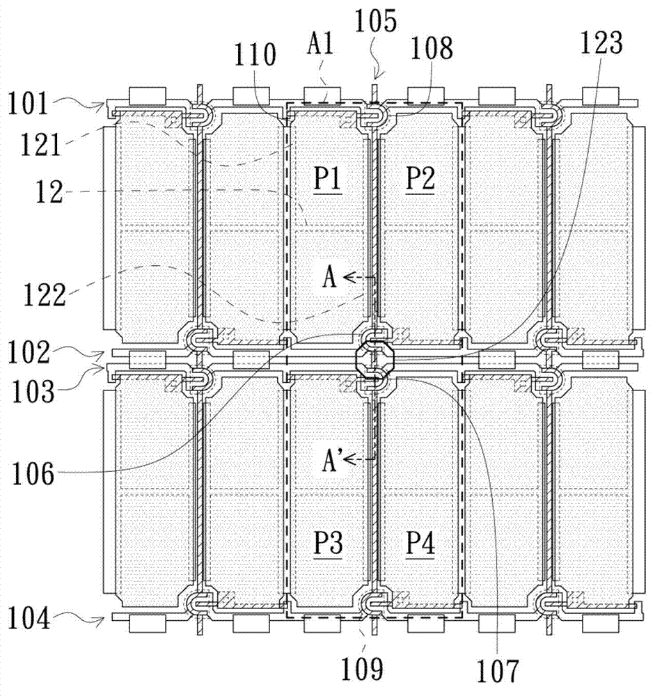
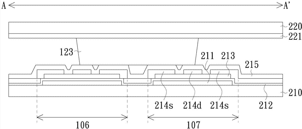
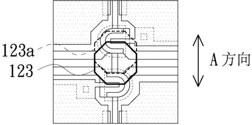
[0047] The first embodiment of the present invention relates to the spacer structure in the Half Source Driver (Half Source Driver) liquid crystal display. The structure of this embodiment can be as follows figure 1 The schematic diagram of the half-source-driven liquid crystal display pixel shown, and figure 2 The schematic diagram of the cross-sectional area of ​​the A-A' marking line shown, figure 1 The area A1 inside the dotted line can be defined as a pixel unit, which is composed of four pixels: P1, P2, P3, and P4. To achieve half-source driving, the four pixels share a data line 105 and are individually driven by the first gate line 101 , the second gate line 102 , the third gate line 103 , and the fourth gate line 104 . Taking the first pixel P1 as an example, the pixel P1 includes a switching element on the array substrate. The switching element can be a thin film transistor 108 as shown in the figure. The gate line 101 controls the opening or closing of the thin fi...


PUM


Abstract

A liquid crystal display panel comprises a first substrate, a second substrate and a spacer. The first substrate comprises a plurality of pixel units. Each pixel unit at least comprises two gate lines and two film transistors connected with the two gate lines. The second substrate is opposite to the first substrate. The spacer is disposed between the first substrate and the second substrate. The spacer overlaps at least one part of the first film transistors and at least one part of the second film transistors in the vertical projection direction.

Description

technical field [0001] The present invention relates to a liquid crystal display panel, and in particular to a liquid crystal display panel capable of avoiding the problem of light leakage and simultaneously improving the light transmission efficiency of the panel. Background technique [0002] The liquid crystal display panel mainly includes an array substrate, a color filter substrate, and a liquid crystal layer arranged between the array substrate and the color filter substrate. In order to maintain the cell gap between the array substrate and the color filter and withstand external pressure, a spacer is placed between the two substrates of the liquid crystal display panel, but a light-shielding layer needs to be placed above the spacer to block the gap. The stray light emitted by the uncontrolled liquid crystal around the object will instead cause the light-transmitting area of ​​the pixel to shrink, and the light efficiency of the liquid crystal display panel will decre...

Claims


Application Information

Patent Timeline
Patent Type & Authority Applications(China)
IPC IPC(8): G02F1/1339
CPCG02F1/133512G02F1/13394G02F1/1368
Inventor 王浚泯沈崇民林建宏
Owner AU OPTRONICS CORP
Why Eureka
Try Eureka