Touch panel and touch component
A touch panel and touch component technology, applied in the direction of instruments, electrical digital data processing, data processing input/output process, etc., can solve the problems of breeding bacteria, affecting the appearance and user experience, residues, etc., to achieve beautiful appearance, Good touch and user experience effects, reducing the effect of seams
- Summary
- Abstract
- Description
- Claims
- Application Information
AI Technical Summary
Problems solved by technology
Method used
Image

Examples
Embodiment 1
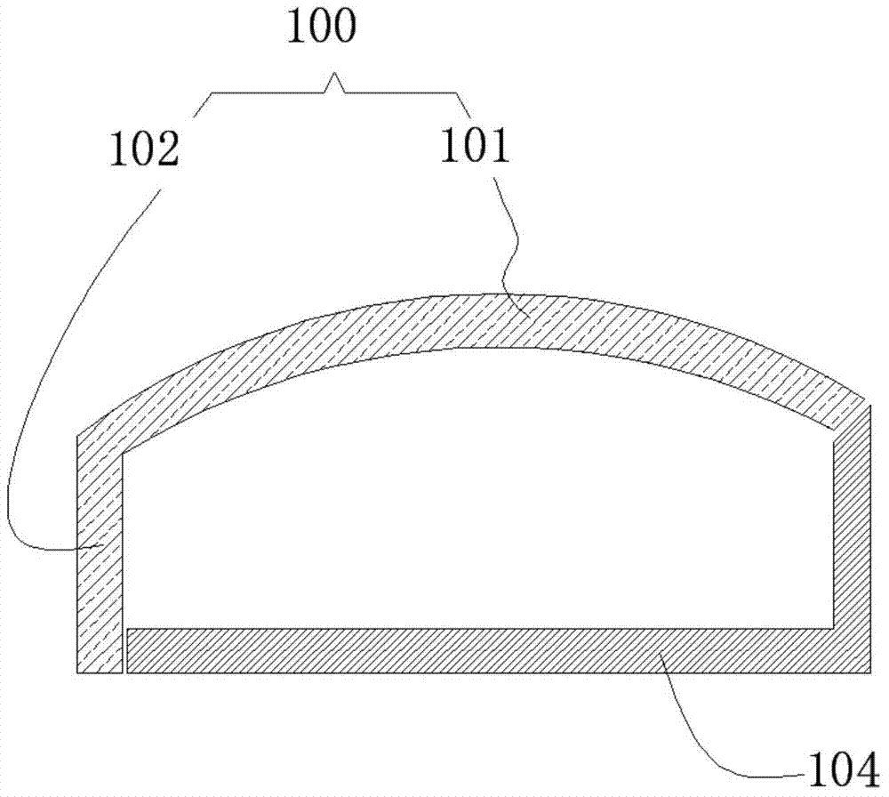
[0038] Such as figure 2 As shown, the touch panel 100 of this embodiment includes an arched top plate 101 and a side plate 102, wherein the side plate 102 is a flat plate, which is integrally formed with the arc-shaped top plate 101 and along the arc-shaped top plate 101 A side in the longitudinal direction extends vertically downward toward the inner side of the arc-shaped top plate 101 .
[0039] Wherein, the thickness of the arched top plate 101 and the side plate 102 is the same, the thickness is 0.3mm-1.0mm, and the width of the arched top plate 101 is 20mm-200mm, and the width of the side plate 102 is 2mm -20mm, the length of the touch panel 100 is 20mm-200mm.
[0040] The material of the touch panel in this embodiment (that is, the arched top plate 101 and the side plate 102) is glass, which can be made by injection molding, which specifically includes: heating the glass to a molten state, injecting it into a low-temperature mold, and cooling it to shape, wherein Con...
Embodiment 2
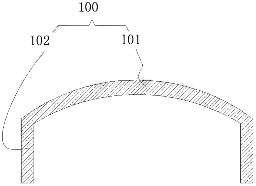
[0044] Such as image 3 As shown, the touch panel 100 of this embodiment includes an arched top plate 101 and two side plates 102, wherein the two side plates 102 are both flat and integrally formed with the arched top plate 101, and the two side plates 102 Extend vertically downward from two opposite sides of the arched top plate 101 in the longitudinal direction to the inner side thereof. The material of the touch panel in this embodiment is polycarbonate, which can be made by injection molding or thermocompression molding. In this embodiment, the two side panels 102 are arranged opposite to each other, which can be used to engage a casing of the electronic device and further reduce seams at the edge of the top panel 101 .
Embodiment 3
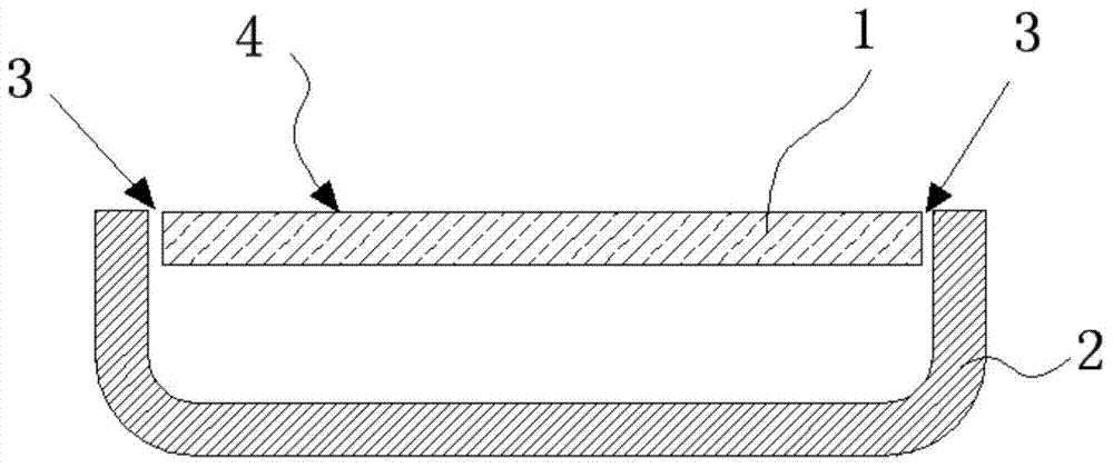
[0046] Such as Figure 4 As shown, the touch panel 100 of this embodiment is further provided with a light-shielding layer on the basis of the touch panel of the second embodiment, specifically including: setting on the inner side of one of the two side panels 102 of the touch panel of the second embodiment The light shielding layer 103 is used for shielding the internal structure of the electronic device from the side.
[0047] In other embodiments, the light-shielding layer 103 may also be provided on the two side boards.
PUM
| Property | Measurement | Unit |
|---|---|---|
| Line width | aaaaa | aaaaa |
Abstract
Description
Claims
Application Information