Packaging structure and method of OLED device

A technology of encapsulation structure and encapsulation method, which is applied in the manufacture of electric solid-state devices, semiconductor devices, semiconductor/solid-state devices, etc., can solve problems such as device failure, prolong service life, prevent water vapor and oxygen from entering OLED devices, and provide good barrier performance effect

Active Publication Date: 2014-01-08
BOE TECH GRP CO LTD
View PDF6 Cites 10 Cited by
  • Summary
  • Abstract
  • Description
  • Claims
  • Application Information

AI Technical Summary

Problems solved by technology

For example, the OLED device is a DC current driven device. When the OLED device is in working condition, if there is water vapor inside the device, a miniature electrolyt

Method used


Image

  • Packaging structure and method of OLED device
  • Packaging structure and method of OLED device
  • Packaging structure and method of OLED device

Examples


Example Embodiment

[0036] The technical solutions in the embodiments of the present invention will be clearly and completely described below with reference to the accompanying drawings in the embodiments of the present invention. Obviously, the described embodiments are only a part of the embodiments of the present invention, but not all of the embodiments. Based on the embodiments of the present invention, all other embodiments obtained by those of ordinary skill in the art without creative efforts shall fall within the protection scope of the present invention.

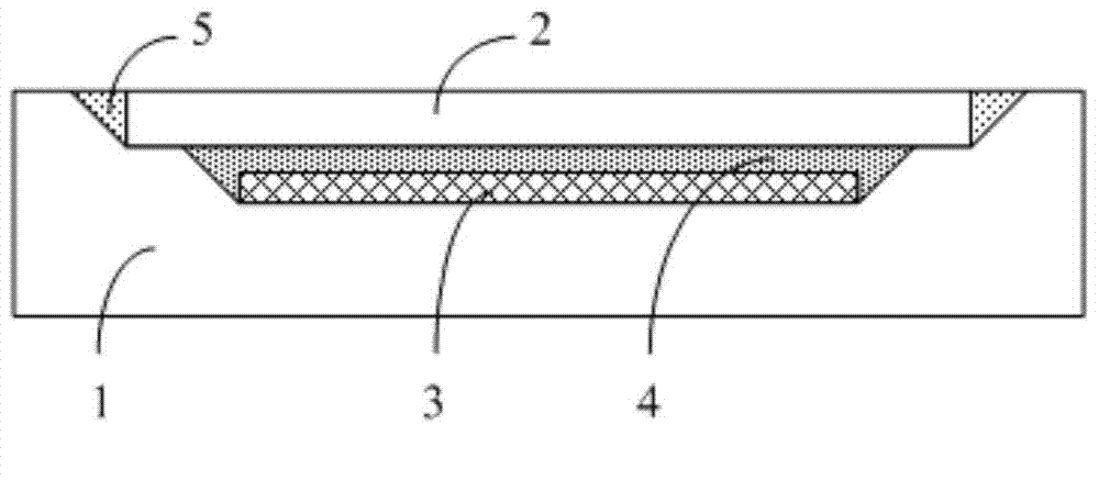
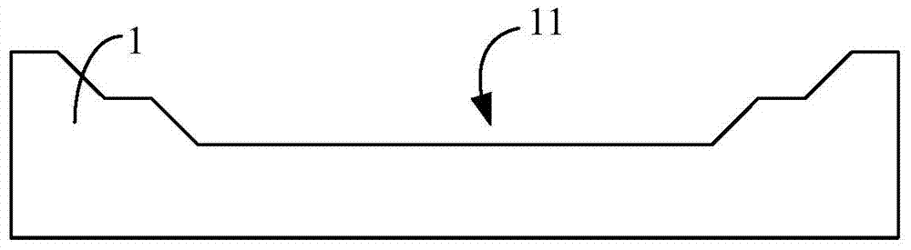
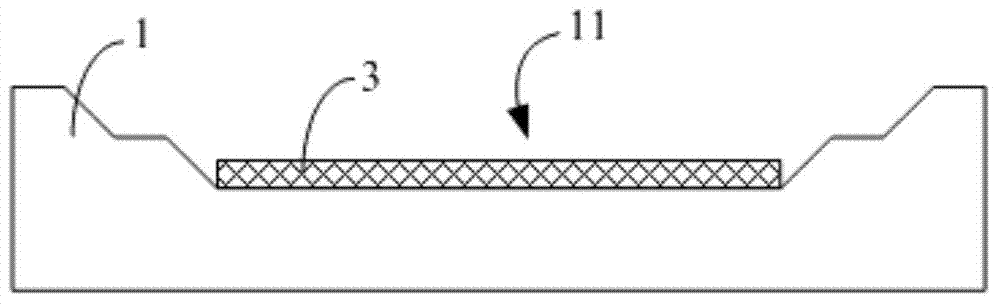
[0037] Please refer to figure 1 , Figure 2a and image 3 ,in, figure 1 It is a schematic structural diagram of the OLED device disposed on the bottom surface of the concave portion of the glass substrate in the packaging structure of the OLED device provided by the embodiment of the present invention; Figure 2a A schematic structural diagram of a glass substrate in the packaging structure of the OLED device provided by the embodi...


PUM


Abstract

The invention relates to the technical field of packaging, and discloses a packaging structure and method of an OLED device. The packaging structure of the OLED device comprises a glass substrate, a glass cover plate, the OLED device and a sealing layer, wherein a sunken portion is arranged on the glass substrate, the glass cover plate is arranged on an opening of the sunken portion, the periphery of the glass cover plate is in bonding with the glass substrate through a glass retaining wall which is formed by glass powder in a melting mode so that the glass cover plate and the glass substrate are of an integrated structure, a closed containing cavity is formed by the glass cover plate and the sunken portion, and the OLED device and the sealing layer are arranged in the closed containing cavity. According to the packaging structure of the OLED device, full-glass packaging of the OLED device is achieved, glass materials can well obstruct water vapor and oxygen, and can prevent the water vapor and the oxygen from entering the OLED device, and the service life of the OLED device is prolonged.

Description

technical field [0001] The invention relates to the field of packaging technology, in particular to a packaging structure and a packaging method of an OLED device. Background technique [0002] OLED devices refer to electroluminescent devices in which organic semiconductor materials and luminescent materials emit light through carrier injection and recombination driven by an electric field. OLED devices have many advantages and have bright prospects in the display field. OLED devices are very sensitive to water vapor and oxygen, and the water vapor and oxygen that penetrate into the OLED device are the main factors that affect the life of the OLED device. Water vapor and oxygen will chemically react with organic materials, causing OLED devices to fail. For example, the OLED device is a DC current driven device. When the OLED device is in working condition, if there is water vapor inside the device, a miniature electrolytic cell will be formed inside the device, and an elec...

Claims


Application Information

Patent Timeline
IPC IPC(8): H01L51/50H01L51/52H01L51/56
CPCH10K50/8426H10K50/841H10K71/00
Inventor 张玉欣
Owner BOE TECH GRP CO LTD
Why Eureka
Try Eureka