

Optical waveguide chip and PD array lens coupling device
A technology of array lens and coupling device, which is applied in the field of optical communication, can solve the problems of inability to use optical fiber group coupling, difficult operation, low production efficiency, etc., and achieves the effects of easier realization of assembly process, lower cost and simple structure
- Summary
- Abstract
- Description
- Claims
- Application Information
AI Technical Summary
Problems solved by technology
Method used
Image

Examples
Embodiment Construction
[0040] The present invention will be described in detail below in conjunction with the accompanying drawings.
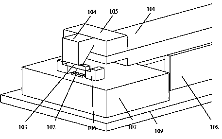
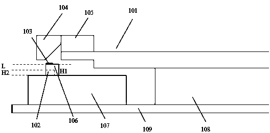
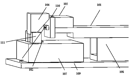
[0041] like figure 1 As shown, it is used for optical waveguide chip and PD array lens coupling structure, including waveguide chip 101, PD array 102, lens array 103, reflective prism 104, cover glass 105, lens holder 106, heat sink 107, waveguide gasket 108, Substrate 109. figure 1The shown heat sink 107 is located on the substrate 109, and the PD array 102 is pasted on the heat sink 107 by conductive glue. The heat sink 107 is provided with a lens holder 106. The lens holder 106 is a combination of two holders, and the two holders are divided into two parts. They are arranged on both sides of the PD array 102; the lens holder 106 is erected with a strip-shaped lens array 103, and the lens array 103 is first fixed on the lens holder 106, and the material of the lens holder 106 is glass. Paste the lens array 103 with the lens holder 106 directly above the PD array ...
PUM
 Abstract
Description
Claims
Application Information