Semiconductor component and its manufacturing method

A semiconductor and component technology, applied in semiconductor/solid-state device manufacturing, semiconductor devices, semiconductor/solid-state device components, etc., can solve discontinuous problems

Active Publication Date: 2016-08-10
ADVANCED SEMICON ENG INC
View PDF4 Cites 0 Cited by
  • Summary
  • Abstract
  • Description
  • Claims
  • Application Information

AI Technical Summary

Problems solved by technology

[0005] In view of this, the present invention provides a semiconductor component made of a wafer and a manufacturing method thereof, so as to solve the existing discontinuous problem of electroplating on the surface of the passivation layer

Method used


Image

  • Semiconductor component and its manufacturing method
  • Semiconductor component and its manufacturing method
  • Semiconductor component and its manufacturing method

Examples


Embodiment Construction

[0021] The description of the following embodiments refers to the attached drawings to illustrate specific embodiments that the present invention can be implemented. Furthermore, the directional terms mentioned in the present invention, such as up, down, top, bottom, front, back, left, right, inside, outside, side, surrounding, center, horizontal, horizontal, vertical, vertical, axial, The radial direction, the uppermost layer or the lowermost layer, etc., are only the direction of reference to the attached drawings. Therefore, the directional terms used are used to describe and understand the present invention, rather than to limit the present invention.

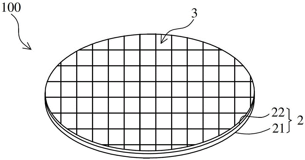
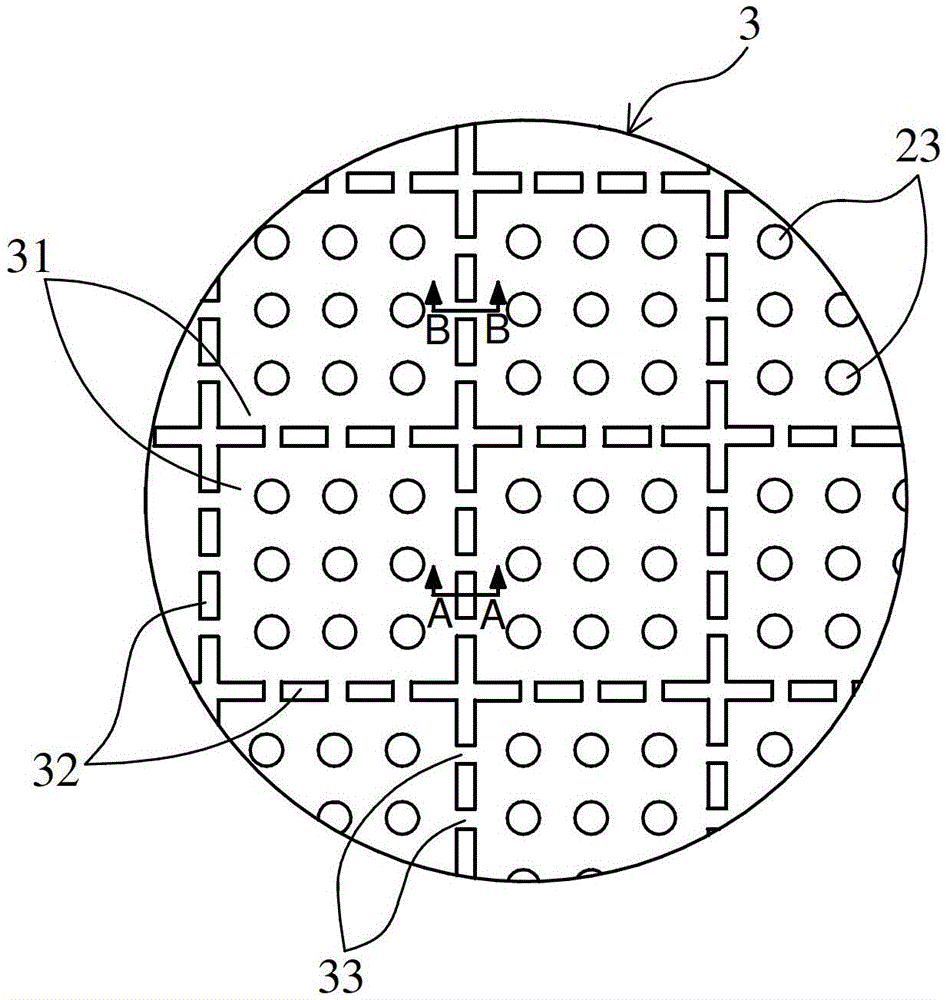
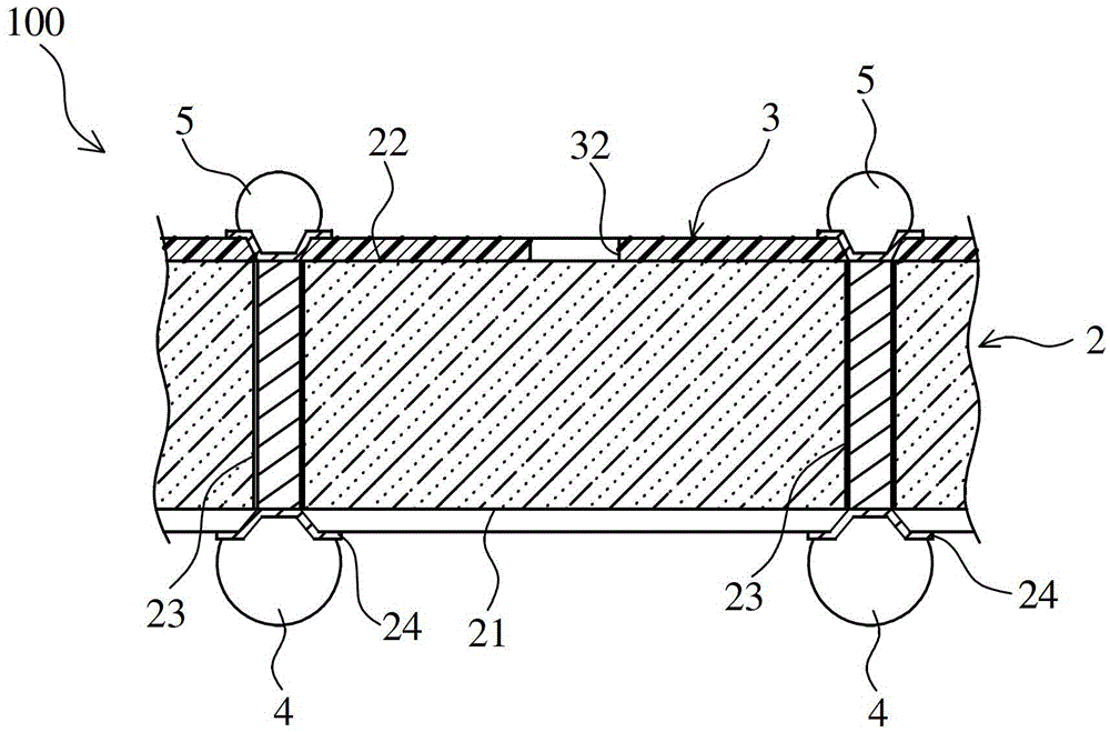
[0022] Please refer to figure 1 , 2 As shown, a semiconductor device 100 according to an embodiment of the present invention mainly includes a semiconductor substrate 2 and at least one passivation layer 3 (Passivation), such as epoxy, benzocyclobutene (BCB, benzocyclobutene) or poly Polyimide (PI), the semiconductor componen...


PUM


Abstract

The invention discloses a semiconductor component and a manufacturing method thereof. The semiconductor component comprises a semiconductor substrate and at least one passivation layer, and the passivation layer comprises several rectangular units, several dicing lines and several bridging parts. The rectangular units are spaced apart from each other, each cutting line is located between two adjacent rectangular units, and the bridging parts are spaced apart from each other across the cutting lines and connect the two adjacent rectangular units. By providing a bridging portion across the cutting line, the surfaces of two adjacent rectangular units can be joined by the bridging portion to achieve the effect of surface continuity, so that the subsequent electroplating path can be connected to all the rectangular units of the passivation layer, To improve the yield of electroplating.

Description

Technical field [0001] The present invention relates to a semiconductor component and a manufacturing method thereof, in particular to a semiconductor component with a bridge portion across a cutting line and a manufacturing method thereof. Background technique [0002] The existing Through Silicon Via (TSV) technology is to arrange vertical circuits in a silicon substrate to provide a 3D circuit structure with higher area density and no side wiring. In the manufacturing process of Through Silicon Via , The silicon substrate is first etched through holes, and then filled with metal conductors such as copper (Cu), silver (Ag), gold (Au), etc., when the through silicon through holes are formed, then the passivation layer is covered to serve as the silicon substrate and the conductor Insulating material between. [0003] With the miniaturization of semiconductor manufacturing processes, the openings made by through silicon vias are getting smaller and smaller, and the passivation lay...

Claims


Application Information

Patent Timeline
Patent Type & Authority Patents(China)
IPC IPC(8): H01L23/48H01L21/768
CPCH01L2224/11
Inventor 郑斌宏
Owner ADVANCED SEMICON ENG INC
Why Eureka
Try Eureka