Light guided pixel

A light guide and pixel technology, which is applied in the direction of optical waveguide light guide, coupling of optical waveguide, semiconductor devices, etc., can solve problems such as reducing the resolution of fluorescent images

Inactive Publication Date: 2014-01-22
CALIFORNIA INST OF TECH
View PDF5 Cites 6 Cited by
  • Summary
  • Abstract
  • Description
  • Claims
  • Application Information

AI Technical Summary

Problems solved by technology

Diffraction, interference, and scattering of weak emitted light signals in filters can degrade fluorescence image resolution

Method used


Image

  • Light guided pixel
  • Light guided pixel
  • Light guided pixel

Examples


Embodiment Construction

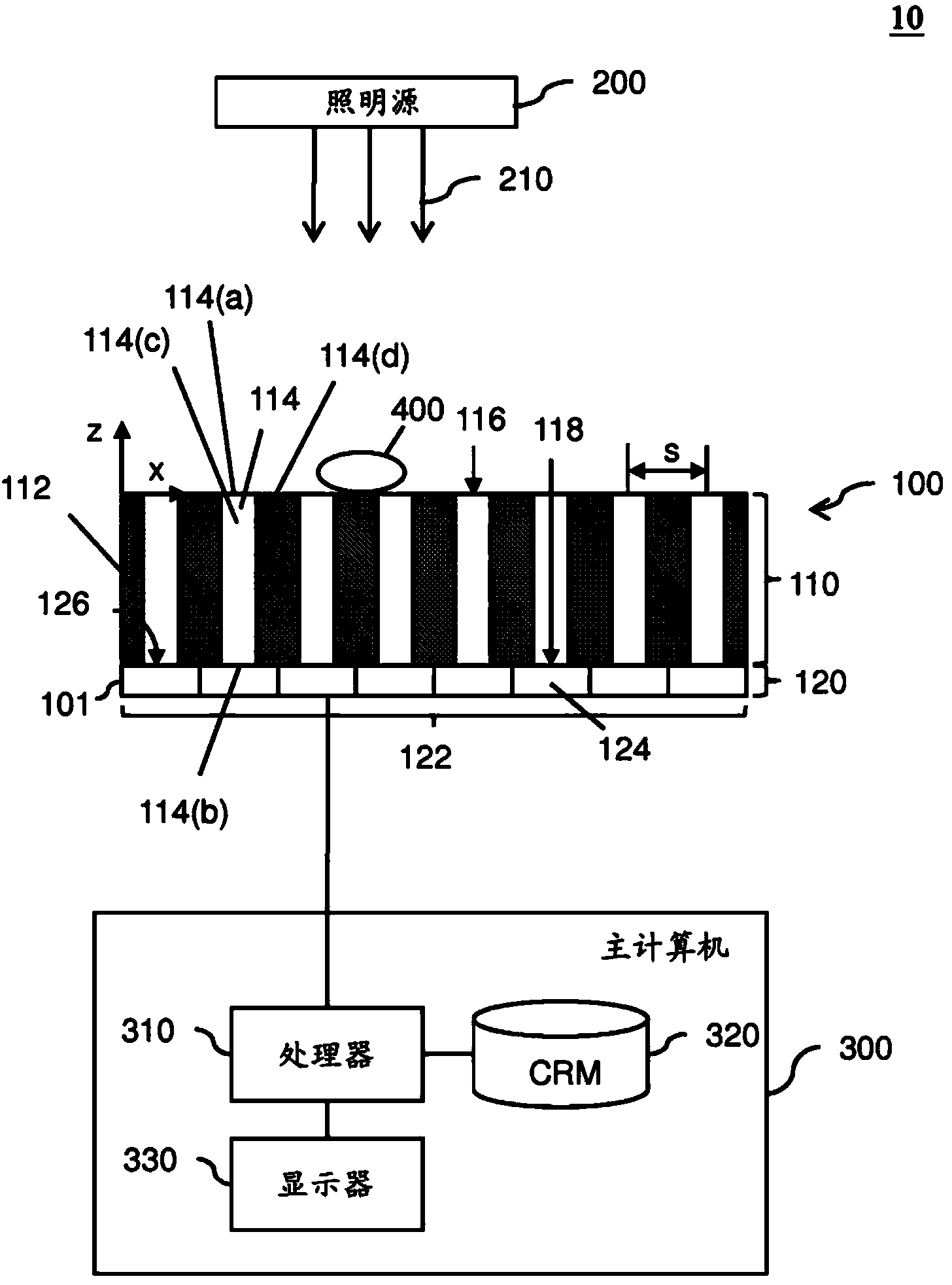
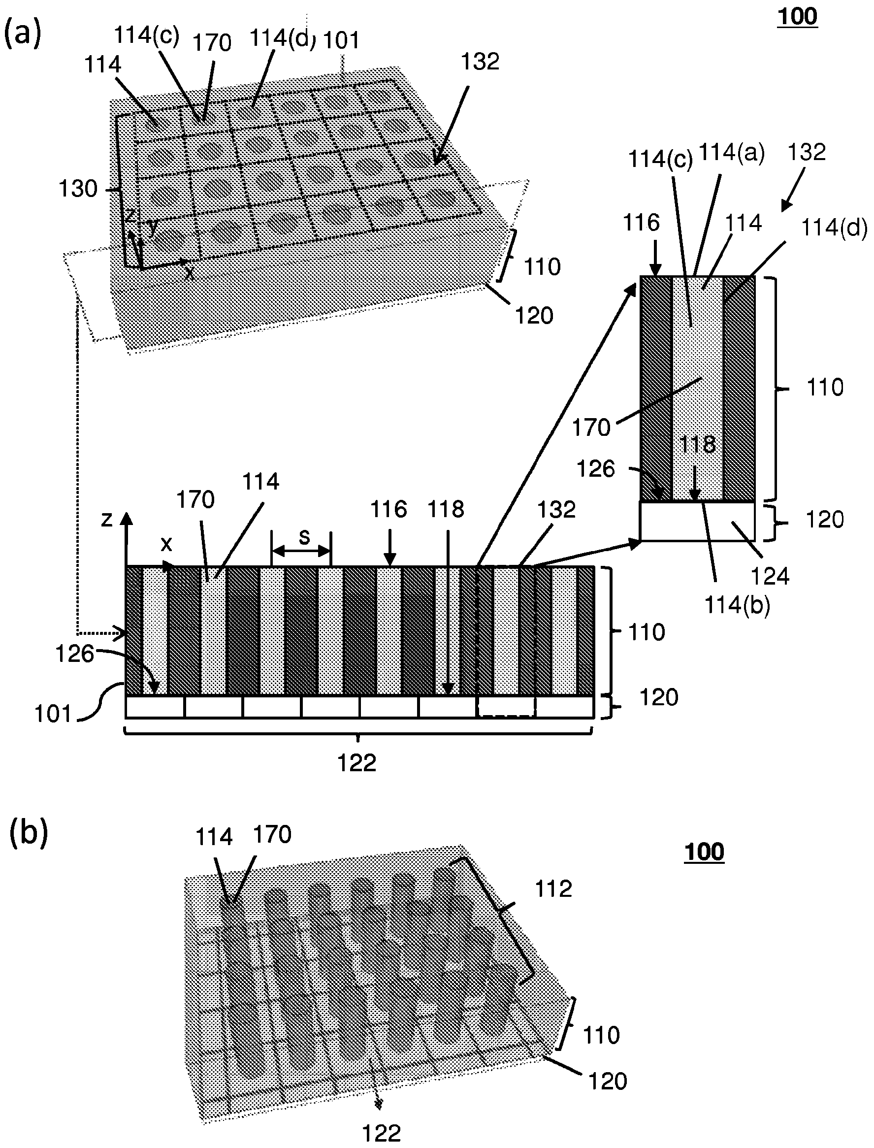
[0025] Embodiments of the present invention will be explained below with reference to the drawings. Embodiments are directed to a light-guiding pixel device having a guiding layer having a plurality of lightguides and a light-detecting layer having a plurality of light-detecting elements (eg, image sensor pixels). Each light guide directs light toward a corresponding light detecting element in the light detecting layer. In one case, each light detecting element of the plurality of light detecting elements receives light from a single light guide. The light guide may also include filters to suppress excitation light and pass emission light. By directing light from locations near the sample, light guides reduce scatter, diffraction, and diffusion, which can improve resolution. The inter-pixel spacing between the lightguides can also improve resolution by separating the light from each lightguide to reduce overlap with adjacent photodetection elements.

[0026] In operation, a...


PUM


Abstract

A light guided pixel having a guide layer and a light detector layer. The guide layer has a light guide. The light detector layer has a light detecting element that receives light channeled by the light guide. The light guide may include a filter for channeling emissions to the light detecting element.

Description

[0001] Cross References to Related Applications [0002] This application is a non-provisional application of U.S. Provisional Patent Application No. 61 / 448,964 entitled "Electronic petridish with bright field and fluorescence imaging capabilities for cell culture monitoring" filed on March 3, 2011 and claims priority thereof. This provisional application is hereby incorporated by reference in its entirety for all purposes. [0003] This nonprovisional application is related to the following co-pending and commonly assigned patent application, which is hereby incorporated by reference in its entirety for all purposes: Filed October 25, 2011 entitled "Scanning Projective Lensless Microscope System" U.S. Patent Application No. 13 / 281,287. [0004] The following nonprovisional application was filed on the same date and is hereby incorporated by reference in its entirety for all purposes: US Patent Application No. 13 / _______. Background technique [0005] Embodiments of the in...

Claims


Application Information

Patent Timeline
Patent Type & Authority Applications(China)
IPC IPC(8): G02B6/42G02B6/10
CPCG01N21/6456G01N2021/6471H01L27/14621H01L27/14629G02B6/10G02B6/42
Inventor 李承亚郑国安本杰明·朱德克维茨庞硕吴继刚杨昌辉
Owner CALIFORNIA INST OF TECH
Why Eureka
Try Eureka