Method used for eliminating system frequency response influences on photo-carrier radiometry technology semi conducting material characteristic measuring equipment

A technology for photocarrier radiation and material properties, which is applied in the field of eliminating the influence of the system frequency response of the photocarrier radiation technology semiconductor material property measurement device, and can solve the problem of reducing the accuracy and reliability of the measurement of semiconductor material property parameters, and future problems. Accurately and effectively eliminate problems such as eliminating the influence of semiconductor material characteristic measurement, eliminating the influence of system frequency response, and improving accuracy and reliability.

Inactive Publication Date: 2014-01-29
TENGZHOU TENGHAI ANALYTICAL INSTR
View PDF6 Cites 9 Cited by
  • Summary
  • Abstract
  • Description
  • Claims
  • Application Information

AI Technical Summary

Problems solved by technology

In fact, instruments such as detectors and lock-in amplifiers have different frequency response functions for different wavelengths of light, so that the influence of the system f...

Method used


Image

  • Method used for eliminating system frequency response influences on photo-carrier radiometry technology semi conducting material characteristic measuring equipment
  • Method used for eliminating system frequency response influences on photo-carrier radiometry technology semi conducting material characteristic measuring equipment
  • Method used for eliminating system frequency response influences on photo-carrier radiometry technology semi conducting material characteristic measuring equipment

Examples


Embodiment Construction

[0032] Embodiments of the present invention can be more fully understood from the following detailed description, which should be read in conjunction with the accompanying drawings. However, it should be noted that the specific embodiment only provides a description of the measurement of some semiconductor material characteristic parameters, but the present invention is not limited to this specific embodiment, and various Variety.

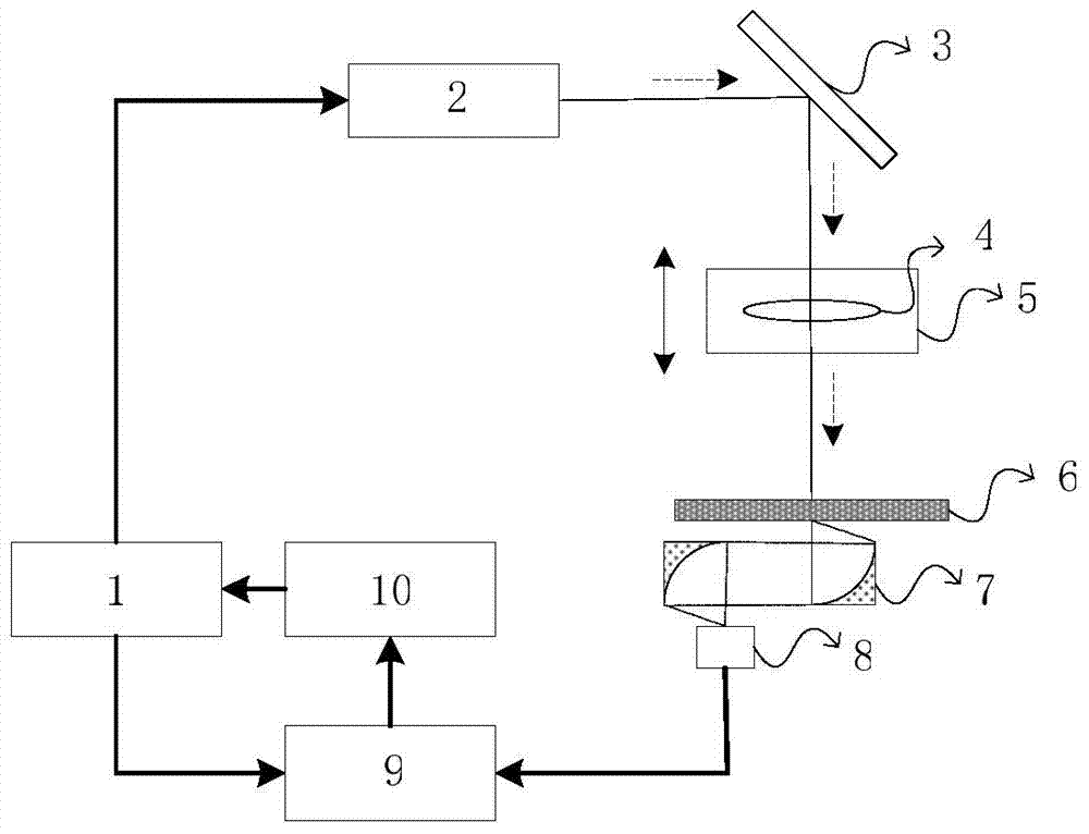
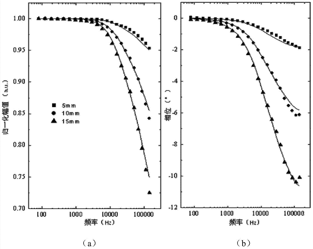
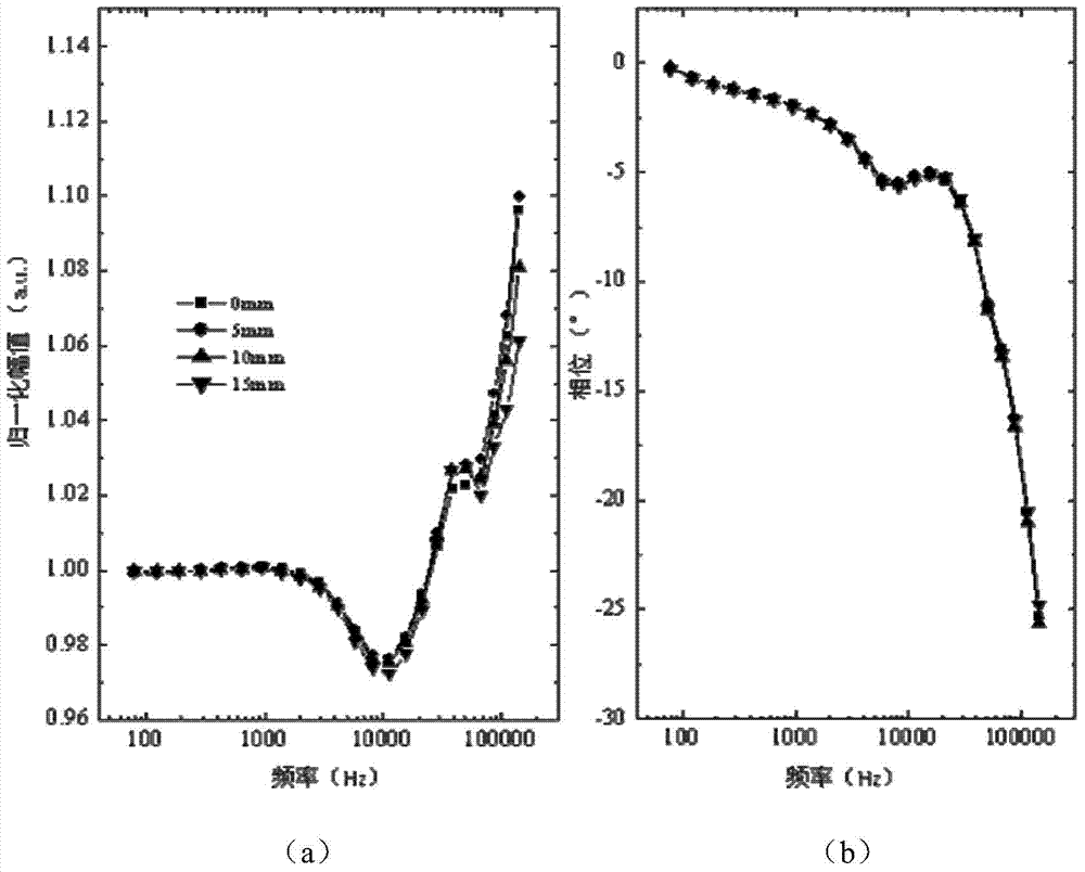
[0033] In the photocarrier radiation technology measurement device, if the influence of the frequency response of the measurement system such as lasers, detectors and lock-in amplifiers cannot be effectively eliminated, the measurement results will deviate from the true value, thereby reducing the measurement accuracy of the characteristics of semiconductor materials . The real signal of the sample after considering the system frequency response is:

[0034] S PCR - R ...


PUM


Abstract

The invention discloses a method used for eliminating system frequency response influences on photo-carrier radiometry technology semi conducting material characteristic measuring equipment. The method is based on infrared radiation which is generated by a semi conducting material after absorption of focused excitation beams processed by strength periodic modulation; characteristic parameters of the semi conducting material are measured by collecting and measuring photo-carrier radiation signals; a relationship curve of the photo-carrier radiation signals and modulation frequency is obtained by changing the modulation frequency of the strength of the excitation beams; a relationship curve of the photo-carrier radiation signals and the modulation frequency under different excitation beam spot sizes is obtained by changing the space between a focusing lens and a sample; and frequency response function of the measuring equipment is obtained, and the influences of the frequency response function on semi conducting material characteristic measurement is eliminated by analyzing the relationship curve of the photo-carrier radiation signals and the modulation frequency under different excitation beam spot sizes. The method is capable of solving a problem that in traditional method measurement accuracy is influenced by relatively high measuring error, and increasing measuring accuracy of measurement on semi conducting material characteristic parameters.

Description

technical field [0001] The invention relates to eliminating the influence of the system frequency response in the process of measuring the characteristics of semiconductor materials, in particular to a method for eliminating the influence of the system frequency response of the semiconductor material characteristic measuring device of the photocarrier radiation technology. Background technique [0002] With the development of semiconductor raw materials in the direction of large diameter and low defect, the integration level of microelectronic devices continues to increase, which puts forward higher requirements for the processing technology and performance testing of materials. In order to ensure that materials can be used in devices and improve device stability and yield, accurate and rapid on-line monitoring and non-destructive characterization of material properties are required in the material processing process. A photo-carrier radiation (PCR: Photo-Carrier Radiometry)...

Claims


Application Information

Patent Timeline
IPC IPC(8): G01N21/63
Inventor 李斌成王谦
Owner TENGZHOU TENGHAI ANALYTICAL INSTR
Why Eureka
Try Eureka