Micro-defect detection method on silicon steel plate surface based on salient active contour model
An active contour model, defect detection technology, used in optical testing flaws/defects, image data processing, instruments, etc.
- Summary
- Abstract
- Description
- Claims
- Application Information
AI Technical Summary
Problems solved by technology
Method used
Image
Examples
specific Embodiment approach
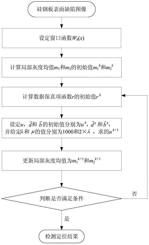
[0096] Such as image 3 As shown, the flow chart of positioning and detection of the method of combining the salient active contour model of an embodiment of the present invention, the specific implementation is as follows:
[0097] Step 3-1. Set the window function W k (x), the window used here is the widely used Gaussian window, the value of σ is 3, and the window size is 4σ+1.
[0098] Step 3-2, the local window function W k (x) into the following formula to get the local gray mean value: the gray mean value of pixels within the curve m 1 and the average gray value of pixels outside the curve m 2 The initial value of m 1 k and m 2 k , where φ is the level set function.
[0099] m 1 =mean(S∈({x∈Ω|φ(x)k (x)))
[0100] m 2 =mean(S∈({x∈Ω|φ(x)>0}∩W k (x)))
[0101] Step 3-3, put m 1 k and m 2 k Bring it into the following formula to get the initial value r of the data fidelity function r k , where k is the number of iterations, and S(x) represents the pixel dat...
PUM
 Abstract
Description
Claims
Application Information


