
Memory device and method making same

A storage device and storage element technology, applied in information storage, static storage, digital storage information, etc., can solve problems such as being unsuitable for miniaturization

Active Publication Date: 2014-02-12
MACRONIX INT CO LTD
View PDF4 Cites 0 Cited by
  • Summary
  • Abstract
  • Description
  • Claims
  • Application Information

AI Technical Summary

Problems solved by technology

Such techniques can use advanced lithographic tools or multiple patterning processes to produce smaller diode sizes and are therefore not suitable for scaling

Method used


Image

  • Memory device and method making same
  • Memory device and method making same
  • Memory device and method making same

Examples


Embodiment Construction

[0063] The following embodiments of the present invention are described in conjunction with Figures 1 to Figure 18 Be explained. The specification describes preferred embodiments to define the scope of the claims, but is not used to limit the present invention. Those skilled in the art of the present invention should be able to understand that there are still many equal changes under the spirit of the present invention.

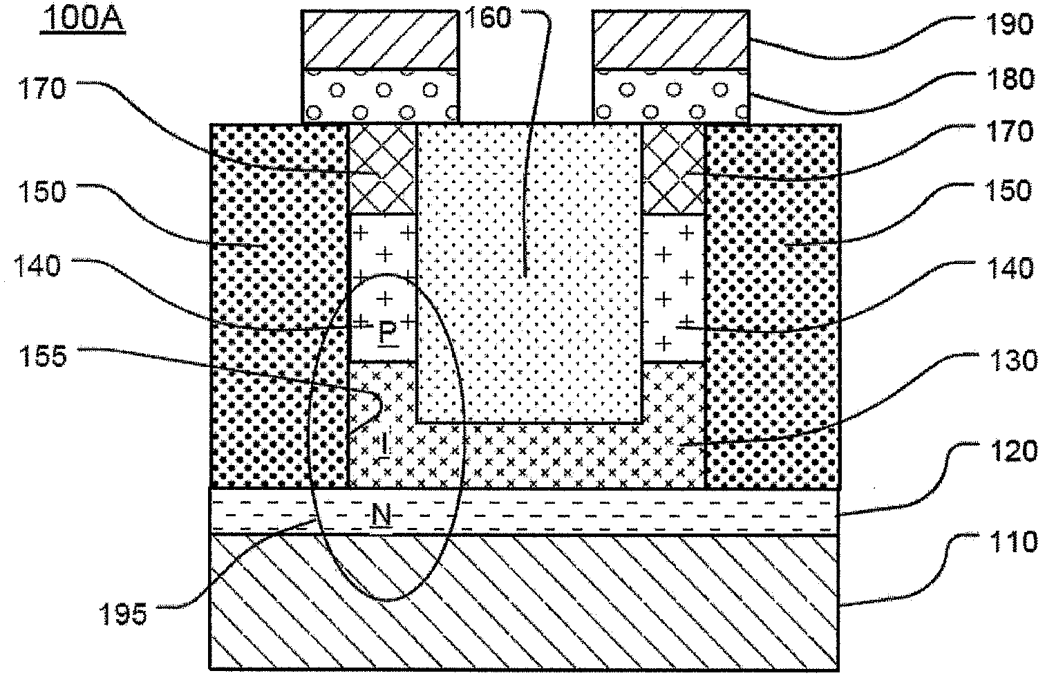
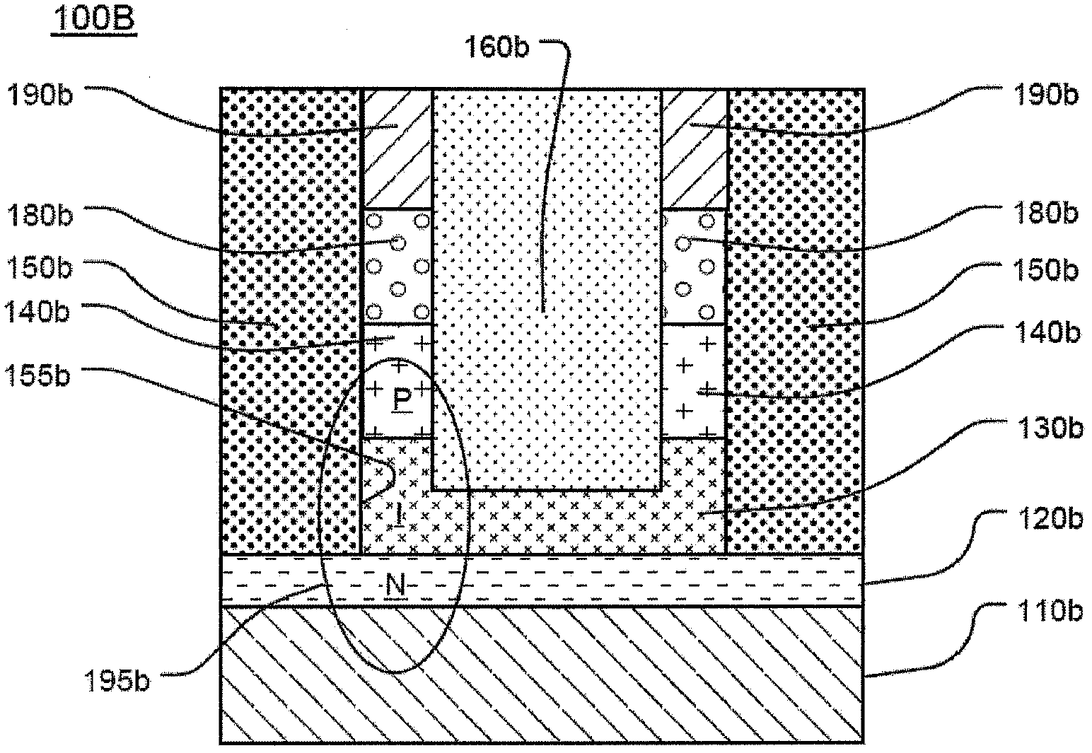
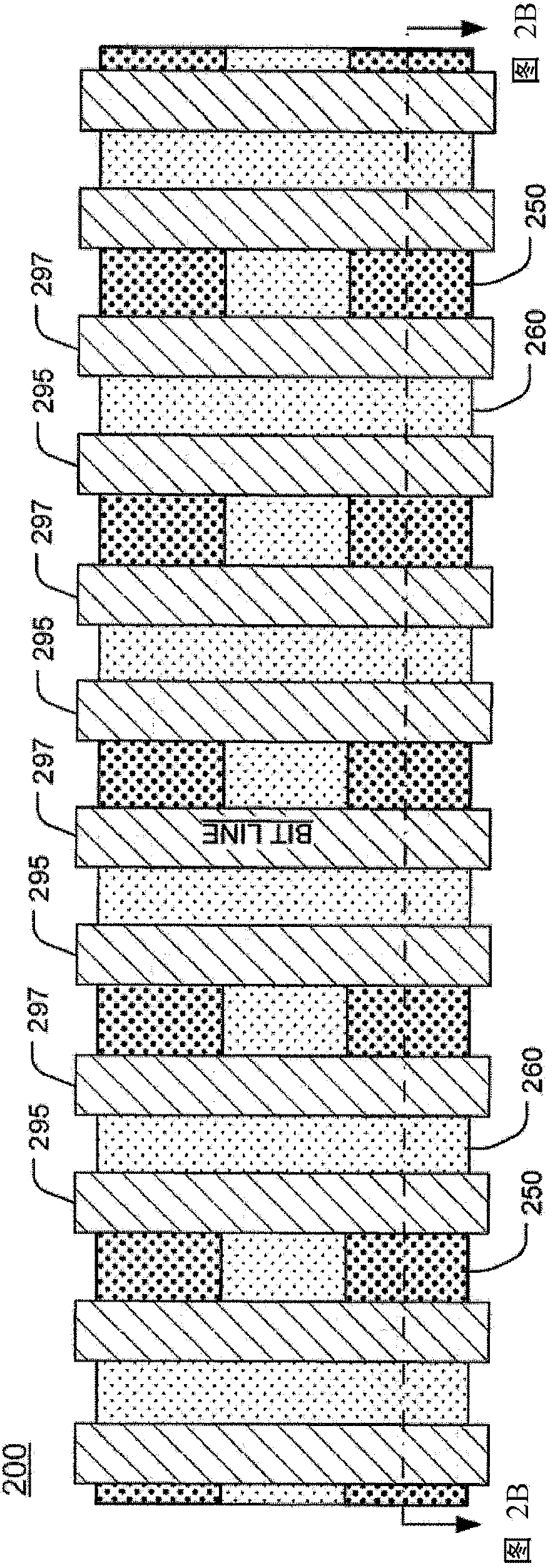
[0064] Here, a sidewall diode driving device used in a memory having a high-density storage device is described. The memory array using the sidewall diode driving device includes a plurality of first access lines, and the first access lines include first conductors. A patterned insulating layer includes a sidewall on the plurality of first access lines. For example, a plurality of channels with first and second sidewalls or other openings can be used in this layer. The sidewall semiconductor is formed on the sidewall. The term "sidewall semiconductor" as use...


PUM


Abstract

A memory device includes a first conductor, a diode, a memory element, and a second conductor arranged in series. The diode includes a first semiconductor layer over and in electrical communication with the first conductor. A patterned insulating layer has a sidewall over the first semiconductor layer. The diode includes an intermediate semiconductor layer on a first portion of the sidewall, and in contact with the first semiconductor layer. The intermediate semiconductor layer has a lower carrier concentration than the first semiconductor layer, and can include an intrinsic semiconductor. A second semiconductor layer on a second portion of the sidewall, and in contact with the intermediate semiconductor layer, has a higher carrier concentration than the intermediate semiconductor layer. A memory element is electrically coupled to the second semiconductor layer. The second conductor is electrically coupled to the memory element.

Description

Technical field [0001] The present invention relates to high-density memory devices based on phase change memory materials such as chalcogenide and other programmable resistance memory materials, and methods for manufacturing such devices. Background technique [0002] In some programmable resistance memory array configurations, each memory cell includes a diode in series with a phase change memory element. The diode is used as a driving element, so that the memory cell can be selected when a forward bias voltage is applied to the diode, and the current in the memory cell is blocked by reverse biasing the diode to select the memory cell. This phase change memory element is composed of a phase change material, which has a great difference in resistance between an amorphous state (high resistivity) and a crystalline state (low resistivity). [0003] In the normal operation of a phase change storage element, when a current pulse is applied through the phase change storage element and...

Claims


Application Information

Patent Timeline
Patent Type & Authority Applications(China)
IPC IPC(8): H01L27/24H01L45/00G11C13/00
CPCG11C13/0004G11C2213/72H10B63/20H10B63/80H10N70/231H10N70/20H10N70/826H10N70/011
Inventor 龙翔澜
Owner MACRONIX INT CO LTD
Features
  • Generate Ideas
  • Intellectual Property
  • Life Sciences
  • Materials
  • Tech Scout
  • Unparalleled Data Quality
  • Higher Quality Content
  • 60% Fewer Hallucinations
Learn More