Bad block table storage method and device and NAND gate nonvolatile memory
A non-volatile memory and storage device technology, which is applied in the direction of memory address/allocation/relocation, response error generation, redundancy in operation, data error detection, etc., can solve serious problems and improve utilization rate , improve reliability, and ensure the effect of normal use
- Summary
- Abstract
- Description
- Claims
- Application Information
AI Technical Summary
Problems solved by technology
Method used
Image
Examples
Embodiment Construction
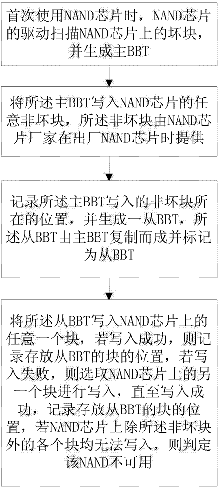
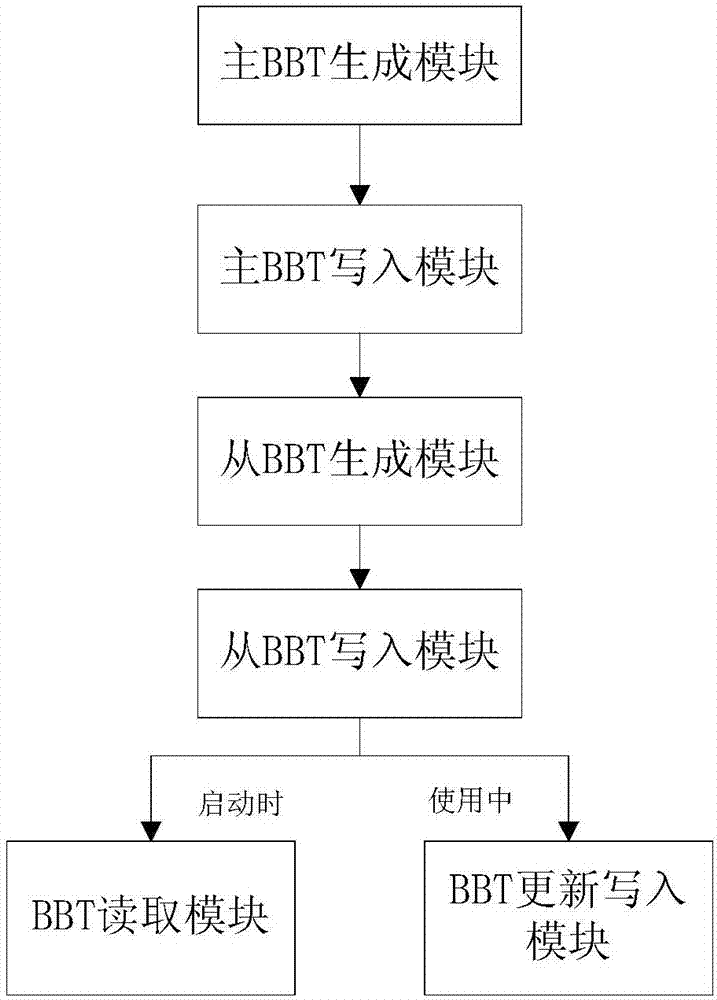
[0035] see figure 1 , a bad block table (English full name: Bad Blocks Table, hereinafter referred to as BBT) storage method, including the following steps:
[0036] Main BBT generation steps: when using the NAND gate non-volatile memory (hereinafter referred to as NAND chip) for the first time, the driver of the NAND chip scans the bad blocks on the NAND chip and generates the main BBT;
[0037] Main BBT writing step: write the main BBT into any non-bad block of the NAND chip, and the non-bad block is provided by the NAND chip manufacturer when the NAND chip leaves the factory. The location of the non-bad block is obtained by querying the data sheet of the NAND chip. Some NAND chip manufacturers guarantee that the first block is a non-bad block, and some NAND chip manufacturers guarantee that the last block is a non-bad block. It cannot be guaranteed that it will always be a non-bad block in future use. Therefore, in this embodiment, the master BBT and the slave BBT are use...
PUM
 Abstract
Description
Claims
Application Information

