Schedule optimization method for communication energy consumption in on-chip network

An on-chip network and optimization method technology, applied in the field of on-chip network, can solve problems such as no optimization method, and achieve the effects of reducing communication distance, energy consumption, and cost

Inactive Publication Date: 2014-03-12
WUHAN UNIV OF SCI & TECH
View PDF5 Cites 7 Cited by
  • Summary
  • Abstract
  • Description
  • Claims
  • Application Information

AI Technical Summary

Problems solved by technology

However, since low-power scheduling is still under development, there is no optimization method disclosed

Method used


Image

  • Schedule optimization method for communication energy consumption in on-chip network
  • Schedule optimization method for communication energy consumption in on-chip network
  • Schedule optimization method for communication energy consumption in on-chip network

Examples


Embodiment 1

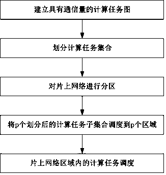
[0046] A scheduling optimization method for communication energy consumption in a network on chip. The steps of the scheduling optimization method are as follows figure 1 Shown:

[0047] Step 1. Establish a computing task graph with communication traffic

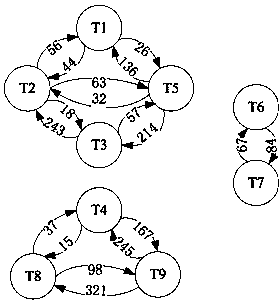
[0048] Obtain the real-time traffic of the computing task when it is running, and establish a computing task graph with the traffic. When the computing task is running, the communication between multiple computing tasks can be obtained through the real-time software monitoring tool, and the specific communication volume can be recorded. According to the communication volume between computing tasks, a computing task graph is established. For example, for the nine computing tasks T1, T2, ..., T9, the traffic is shown in Table 1.

[0049] Table 1 Communication traffic of computing tasks

[0050] T1 T2 T3 T4 T5 T6 T7 T8 T9 T1 - 44 63 0 26 0 0 0 0 T2 56 - 18 0 0 0 0 0 0...

Embodiment 2

[0087]A scheduling optimization method for communication energy consumption in a network on chip. Except step 3 and step 5, all the other are the same as embodiment 1.

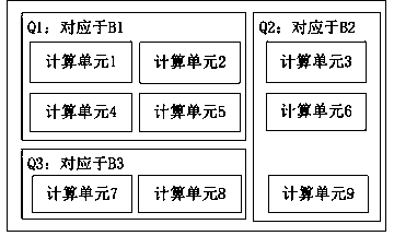
[0088] Step 3. Partition the network on chip

[0089] The specific steps of dividing the on-chip network into p areas according to the p divided computing task sets B:

[0090] Step 3.1. If the number of computing tasks M ≤ the number U of computing units of the network on chip, it should satisfy:

[0091] Area Qj corresponds to the divided computing task set Bj;

[0092] The number of computing units in the area Qj ≥ the number of computing tasks in the divided computing task set Bj;

[0093] Step 3.2. If the number of computing tasks M>the number of computing units U of the network on chip, the method of dividing the network on chip into p areas is as follows:

[0094] i) Select the divided computing task set Bj that contains the largest number of computing tasks from the p divided computing task sets B,...


PUM


Abstract

The invention relates to a schedule optimization method for communication energy consumption in an on-chip network. According to the technical scheme, the method comprises the following steps: with the combination of characteristics of communication in the on-chip network, calculating communication density among different calculation tasks of the on-chip network, and establishing a calculation task diagram with communication traffic; subsequently dividing a calculation task set according to the communication traffic and the mutual relationship among the calculation tasks; furthermore dividing the on-chip network according to the division of the task set; subsequently scheduling the calculation task set into an area; finally performing calculation task scheduling within the area so as to reduce communication energy consumption and achieve the optimization target. By adopting the method, schedule optimization on communication energy consumption in the on-chip network is achieved, high-efficiency distribution on the calculation tasks in the on-chip network is promoted, and the communication energy consumption of the on-chip network is reduced.

Description

technical field [0001] The invention belongs to the technical field of network on chip. Specifically, the invention relates to a scheduling optimization method for communication energy consumption in a network on chip. Background technique [0002] For a long time, processor chip manufacturers have improved the performance of the processor by increasing the main frequency. However, with the continuous improvement of chip manufacturing technology, the traditional processor architecture is already facing a huge bottleneck. The integration level of transistors has reached hundreds of millions, and it is difficult to improve performance simply by increasing the main frequency, and high main frequency also brings high power consumption. From the perspective of application requirements, increasingly complex multimedia, scientific computing, virtualization and other application fields require more powerful computing capabilities. In this context, multi-core processors came into ...

Claims


Application Information

Patent Timeline
Patent Type & Authority Applications(China)
IPC IPC(8): G06F9/48
CPCY02D10/00
Inventor 胡威邹代坤黎文飞张凯郭宏江若成张若凡李伟强谭练薛智文
Owner WUHAN UNIV OF SCI & TECH
Why Eureka
Try Eureka