Image sensor and backlight calibration method thereof

A technology of image sensor and calibration method, which is applied in the field of semiconductors, can solve the problems of black backlight information backlight calibration and inability to obtain high-quality images, etc., to achieve accurate backlight calibration and improve quality

Inactive Publication Date: 2014-03-26
GALAXYCORE SHANGHAI
View PDF4 Cites 3 Cited by
  • Summary
  • Abstract
  • Description
  • Claims
  • Application Information

AI Technical Summary

Problems solved by technology

However, it has been found that the black backlight information cannot be accurately calibrated with the existing image sensor and its backlight calibration method, so the existing image sensor cannot obtain high-quality images

Method used


Image

  • Image sensor and backlight calibration method thereof
  • Image sensor and backlight calibration method thereof
  • Image sensor and backlight calibration method thereof

Examples


Embodiment Construction

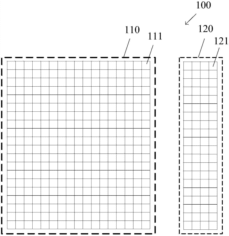
[0038] Please refer to figure 1 , figure 1 It is a schematic top view of an existing image sensor 100 . The existing image sensor 100 includes an effective pixel area 110 and a reference pixel area 120 located at the edge of the effective pixel area 110 . The reference pixel area 120 is used for backlight calibration. The effective pixel area 110 includes a plurality of photosensitive pixel units 111 , and the reference pixel area 120 includes a plurality of photosensitive pixel units 121 . In order to perform accurate backlight calibration, it is necessary to ensure that the reference pixel area 120 is not affected by electrons generated by the effective pixel area 110 .

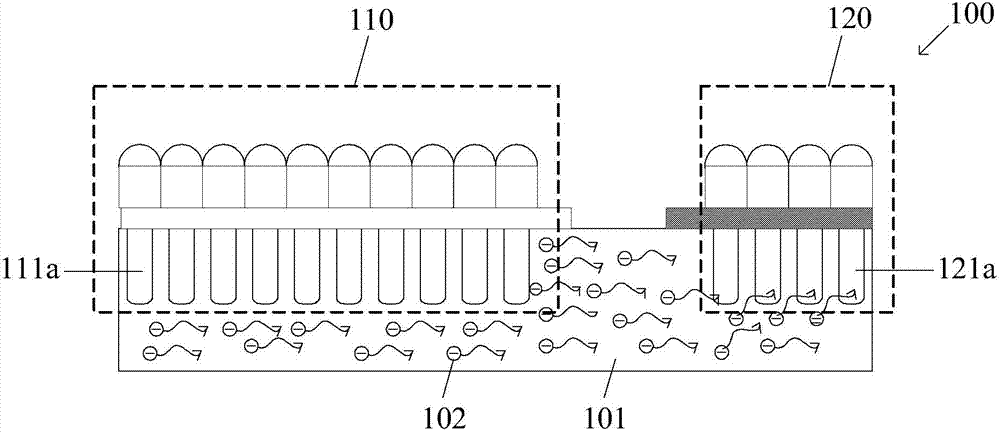
[0039] Please refer to figure 2 , figure 2 It is a schematic diagram of a section of an existing image sensor 100 . In the existing image sensor 100, since the effective pixel area 110 is adjacent to the reference pixel area 120, there is a certain distance between them. This part of the distance is u...


PUM


Abstract

The invention relates to an image sensor and a backlight calibration method of the image sensor. The image sensor comprises an effective pixel area, a reference pixel area and a current carrier dissociation area, wherein the effective pixel area is provided with a plurality of photosensitive pixel units, the reference pixel area is located outside at least one side of the effective pixel area, and the current carrier dissociation area is correspondingly located between the effective pixel area and the reference pixel area. Because the image sensor is provided with the current carrier dissociation area located between the effective pixel area and the reference pixel area, after current carriers in the effective pixel area enter a substrate, the image sensor can dissociate the current carriers form the current carrier dissociation area with the backlight calibration method so as to prevent the current carriers from migrating to the reference pixel area. Thus, accurate backlight calibration can be performed on the image sensor, and thus the quality of images output by the image sensor is improved.

Description

technical field [0001] The invention relates to the technical field of semiconductors, in particular to an image sensor and a backlight calibration method thereof. Background technique [0002] Image sensors are semiconductor devices that convert optical signals into electrical signals. Existing image sensors can be of different types such as complementary metal-oxide-semiconductor (CMOS) image sensors and charge-coupled device (CCD) image sensors. Regardless of the type of image sensor, the image obtained usually needs to undergo black backlight information (black level) backlight calibration (black level calibration) so as to truly reflect the black backlight information. Accurate black backlight information Backlight calibration helps to obtain digital photos with full contrast and subtle details in shadow areas. If the backlight correction is not good, the final output image may appear completely black (too much backlight correction, information is lost) or parts that ...

Claims


Application Information

Patent Timeline
IPC IPC(8): H01L27/146
Inventor 李文强蒋珂玮赵立新
Owner GALAXYCORE SHANGHAI
Why Eureka
Try Eureka