
Method for producing field effect transistor, field effect transistor, display device, image sensor, and x-ray sensor

一种场效晶体管、制造方法的技术,应用在晶体管、辐射控制装置、半导体/固态器件制造等方向,能够解决晶体管阈值偏移等问题

Active Publication Date: 2014-03-26
SAMSUNG DISPLAY CO LTD
View PDF8 Cites 15 Cited by
  • Summary
  • Abstract
  • Description
  • Claims
  • Application Information

AI Technical Summary

Problems solved by technology

Assuming that the optical bandgap of IGZO is relatively narrow and has optical absorption in its region, the following problem will arise, that is, the threshold shift of the transistor will occur

Method used


Image

  • Method for producing field effect transistor, field effect transistor, display device, image sensor, and x-ray sensor
  • Method for producing field effect transistor, field effect transistor, display device, image sensor, and x-ray sensor
  • Method for producing field effect transistor, field effect transistor, display device, image sensor, and x-ray sensor

Examples


Embodiment 1

[0214] First, the TFT of Example 1 was produced by the following production method.

[0215] Figure 9A It is the plan view of the TFT of the embodiment and the comparative example, Figure 9B yes Figure 9A A-A line arrow cross-sectional view of the shown TFT.

[0216] Such as Figure 9A and Figure 9B As shown, a p-type Si substrate 502 (1 inch square, thickness: 525 μmt, thermal oxide film (SiO 2): 100 nmt) As a substrate, a simple TFT 500 using a thermal oxide film 504 as a gate insulating layer was produced.

[0217] The oxide semiconductor layer 505 formed on the substrate 502 is divided into the first oxide semiconductor film 506, the second oxide semiconductor film 507, and the third oxide semiconductor film 508 as described above, and each film is continuous without being exposed to the atmosphere. film formation. The sputtering of each film uses In 2 o 3 Target, Ga 2 o 3 The ternary co-sputtering of target and ZnO target is carried out. The adjustment of ...

Embodiment 2

[0237] The TFT of Example 2 was manufactured using the same manufacturing method as TFT 1 except for the heat treatment step, that is, the heat treatment environment of the third step and the fifth step. Specifically, an atmospheric environment was used as the heat treatment environment in the third step, and an oxidizing environment with an oxygen partial pressure of 100% was used as the heat treatment environment in the fifth step, thereby obtaining the TFT of Example 2.

Embodiment 3

[0239] The TFT of Example 3 was manufactured using the same manufacturing method as TFT 1 except for the heat treatment step, that is, the heat treatment environment of the third step and the fifth step. Specifically, an oxidative environment with an oxygen partial pressure of 100% was used in the third step, and an oxidative environment with an oxygen partial pressure of 100% was used as the heat treatment environment in the fifth step, thereby obtaining the TFT of Example 3.


PUM


Abstract

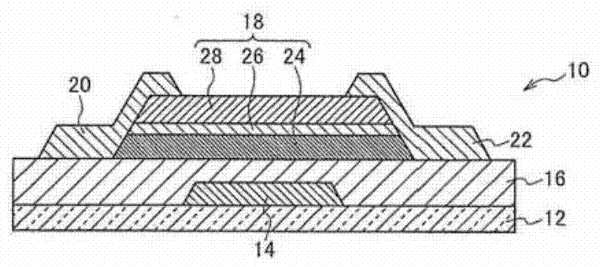
A method for producing field effect transistor stabilizes the TFT characteristics during light irradiation. The method is provided with: a first step for growing a first oxide semiconductor film (24) over a gate insulation layer (16) disposed over a gate electrode (14); a second step for growing a second oxide semiconductor film (26) differing in cation composition from the first oxide semiconductor film (24), and having lower electrical conductivity than the first oxide semiconductor film (24); a third step for heat treatment in excess of 300 C in an oxidizing atmosphere; a fourth step for growing a third oxide semiconductor film (28) differing in cation composition from the first oxide semiconductor film (24), and having lower electrical conductivity than the first oxide semiconductor film (24); a fifth step for heat treatment in excess of 300 C in an oxidizing atmosphere; and an electrode formation step for forming a source electrode (20) and a drain electrode (22) over the third oxide semiconductor film (28).

Description

technical field [0001] The invention relates to a manufacturing method of a field effect transistor, a field effect transistor, a display device, an image sensor and an X-ray sensor. Background technique [0002] In recent years, field-effect transistors have been used as unit elements of integrated circuits for semiconductor memory, high-frequency signal amplification elements, liquid crystal drive elements, etc., and those that have been thinned are used in a wide range of fields as thin film transistors (Thin Film Transistor, TFT). . [0003] As the semiconductor channel layer (active layer) forming field effect transistors, silicon semiconductors or their compounds have been mostly used in the past, and single crystal silicon is used in high-frequency amplifying elements and integrated circuits that require high-speed operation, or although low-speed operation However, amorphous silicon is used in applications such as displays and other liquid crystal drive devices that...

Claims


Application Information

Patent Timeline
Patent Type & Authority Applications(China)
IPC IPC(8): H01L29/786G01T1/24G09F9/30H01L21/336H01L27/144H01L27/146H01L27/32
CPCH01L29/78696H01L27/3244H01L27/14632H01L29/66969H01L27/14659H01L29/66742H01L27/14687H01L27/3248H01L27/1225H01L27/156H01L27/322H01L27/3262H01L29/7869H01L21/02565H01L27/148H01L27/14612H01L27/14614H10K59/38H10K59/123H10K59/1213H01L27/144H10K59/12
Inventor 小野雅司高田真宏望月文彦田中淳铃木真之
Owner SAMSUNG DISPLAY CO LTD
Learn More