Supercharge Your Innovation With Domain-Expert AI Agents!

Wafer Alignment Method for Image Sensor Wafer-Level Test

An image sensor, wafer-level technology, used in semiconductor/solid-state device testing/measurement, electrical components, circuits, etc. Accuracy, difficulty in meeting the alignment accuracy requirements of CMOS image sensors, etc., to achieve the effect of improving accuracy and efficiency

Active Publication Date: 2016-06-29
格科微电子(浙江)有限公司
View PDF4 Cites 1 Cited by
  • Summary
  • Abstract
  • Description
  • Claims
  • Application Information

AI Technical Summary

Problems solved by technology

[0005] However, in the existing process, as the tested CMOS sensor products become smaller and smaller, due to the low alignment accuracy between the test needle card and the solder ball point, it is difficult to meet the alignment accuracy requirements of the wafer-level test of the CMOS image sensor. Therefore, it is impossible to accurately conduct electrical tests on each die in the wafer, which reduces the accuracy of wafer-level testing of CMOS image sensors.

Method used


Image

  • Wafer Alignment Method for Image Sensor Wafer-Level Test
  • Wafer Alignment Method for Image Sensor Wafer-Level Test
  • Wafer Alignment Method for Image Sensor Wafer-Level Test

Examples


Embodiment Construction

[0027] In the following description, numerous specific details are set forth in order to provide a thorough understanding of the present invention. However, the present invention can be implemented in many other ways different from those described here, and those skilled in the art can make similar extensions without violating the connotation of the present invention, so the present invention is not limited by the specific embodiments disclosed below.

[0028] The invention provides a wafer alignment method suitable for wafer-level testing of an image sensor, which can provide higher alignment accuracy and has low implementation complexity.

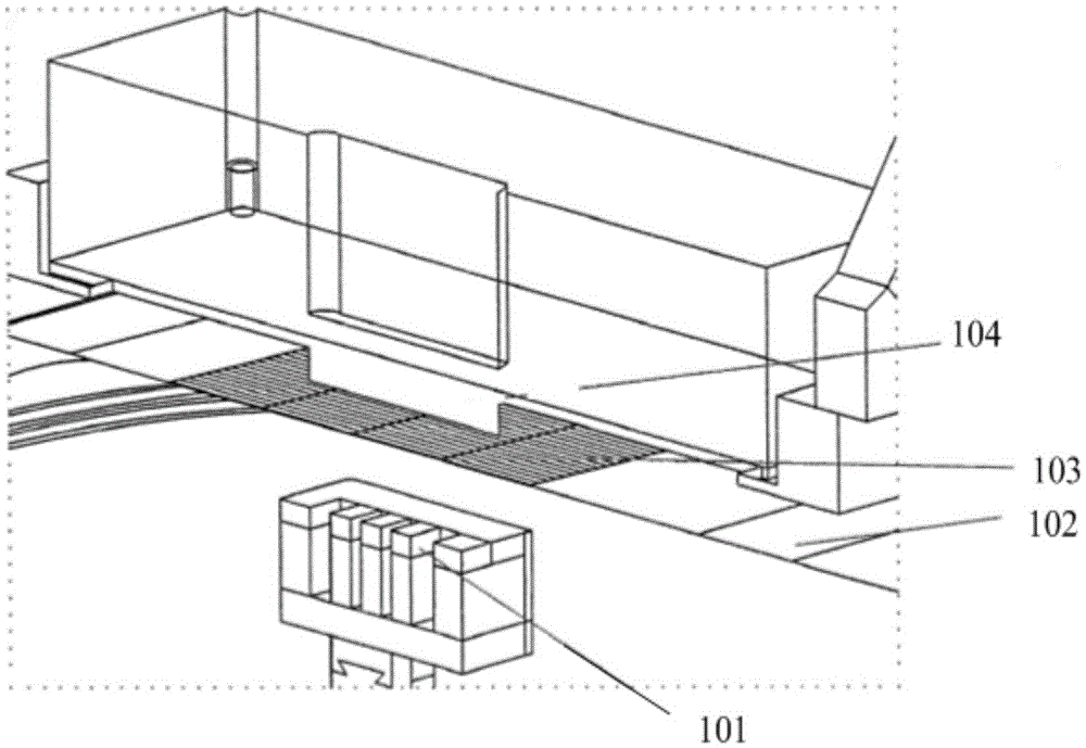
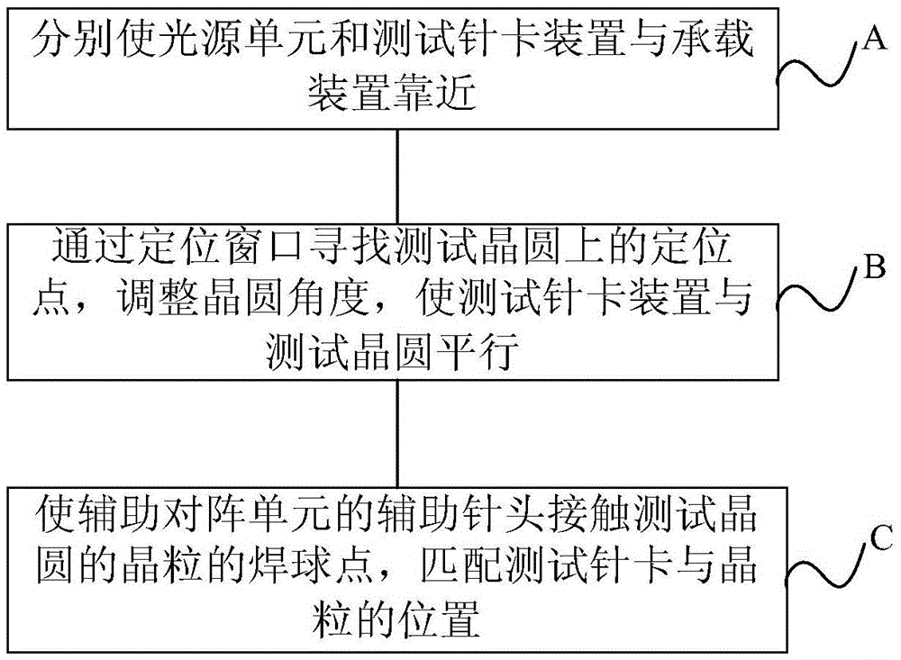
[0029] The alignment method first provides an image sensor wafer-level test device, the test device includes: a light source unit, a test needle card device located on the upper part of the light source unit, and a test wafer carried on a carrier device, the test The photosensitive surface of the wafer is arranged towards the carrying dev...


PUM


Abstract

The invention relates to a wafer aligning method for wafer-level testing of an image sensor. The method comprises the following steps of moving a light source unit or a bearing device in the vertical direction, so as to enable the light source unit and the bearing device to get close in the vertical direction, and enabling a testing probe card device to move downwards in the vertical direction; providing a positioning window arranged on a testing probe card, and providing at least two positioning points in the testing wafer; enabling the testing probe card device to find the positioning point on the testing wafer by the positioning window through a camera, further adjusting the angle of the wafer, enabling the testing probe card device to be parallel with the testing wafer, and matching the position of the testing wafer; providing an auxiliary probe aligning unit which is arranged on the testing probe card device, and enabling at least two auxiliary probe heads of the probe aligning unit to expose out of the lower surface of the testing probe card device; enabling the auxiliary probe heads of the auxiliary probe aligning unit to be in contact with a welding ball point of a wafer particle, and matching the testing probe card device and the position of the welding ball point of the wafer particle, so as to align the testing probe card device and the testing wafer.

Description

technical field [0001] The invention relates to the technical field of semiconductor testing, in particular to a wafer alignment method suitable for wafer-level testing of image sensors. Background technique [0002] CMOS (ComplementaryMetalOxideSemiconductor, Complementary Metal Oxide Semiconductor) image sensor production process is: design, wafer (wafer) production, color filter, CSP (ChipScalePackage, chip-level packaging), testing. In the wafer test step, it is necessary to conduct an electrical test on the die to ensure that the die on the silicon wafer is a qualified product before packaging, so wafer test is one of the key steps to improve the yield of semiconductor devices one. [0003] Generally speaking, the CMOS image sensor products that arrive at the test are cut individual products, but as the size of the CMOS image sensor becomes smaller and smaller, the size of the individual test products becomes smaller and smaller, and the test operation of the individua...

Claims


Application Information

Patent Timeline
Patent Type & Authority Patents(China)
IPC IPC(8): H01L21/66
CPCH01L22/34
Inventor 熊望明赵立新李文强
Owner 格科微电子(浙江)有限公司
Features
  • R&D
  • Intellectual Property
  • Life Sciences
  • Materials
  • Tech Scout
  • Unparalleled Data Quality
  • Higher Quality Content
  • 60% Fewer Hallucinations
Learn More