Image module and manufacturing method thereof

A manufacturing method and image technology, which can be used in image communication, radiation control devices, televisions, etc., can solve problems such as unfavorable product thinning, and achieve the effect of reducing the overall height of the module, the height of the module, and the reduction of bad wear and tear.

Inactive Publication Date: 2014-04-09
BISON ELECTRONICS
View PDF6 Cites 0 Cited by
  • Summary
  • Abstract
  • Description
  • Claims
  • Application Information

AI Technical Summary

Problems solved by technology

However, a plurality of solder balls 25' are formed around the bottom of the glass substrate 21' of the image sensing package 2' of the raw material. If the traditional surface mount process (SMT) method is used, the solder balls 25' are electrically bonded to the The surface of the circuit board 3' will produce a height 1H of the solder ball, which will increase the height H from the top surface of the lens 12' to the bottom surface of the circuit board 3', which is not conducive to the demand for thinner products

Method used


Image

  • Image module and manufacturing method thereof
  • Image module and manufacturing method thereof
  • Image module and manufacturing method thereof

Examples


Embodiment Construction

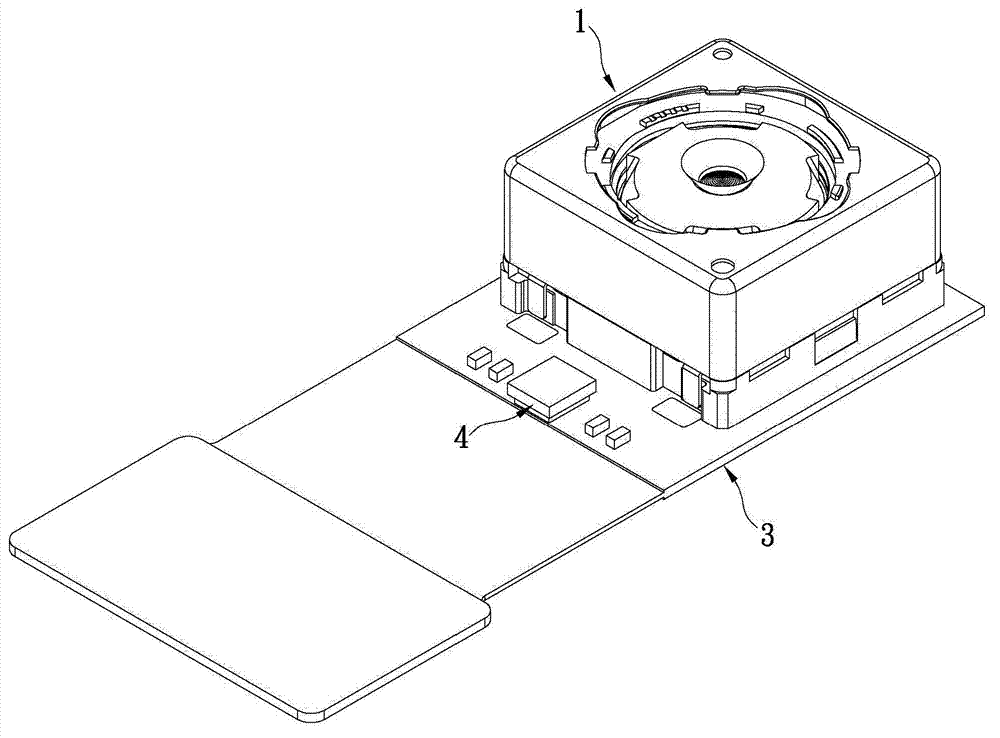
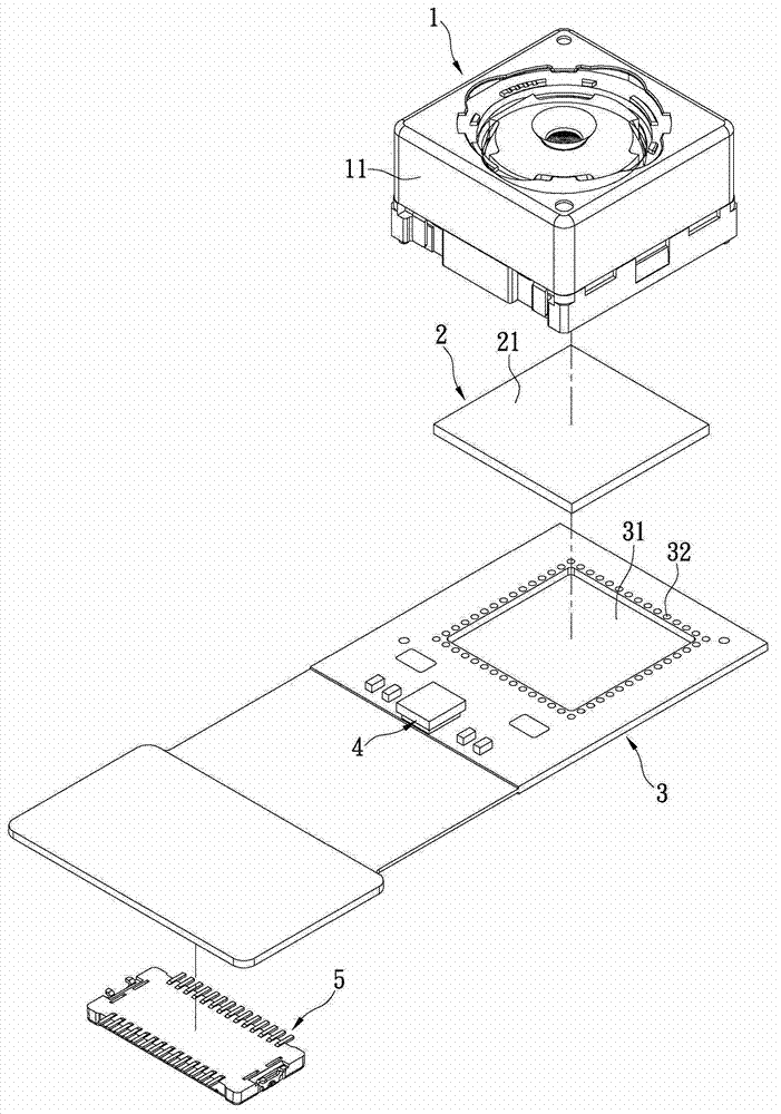
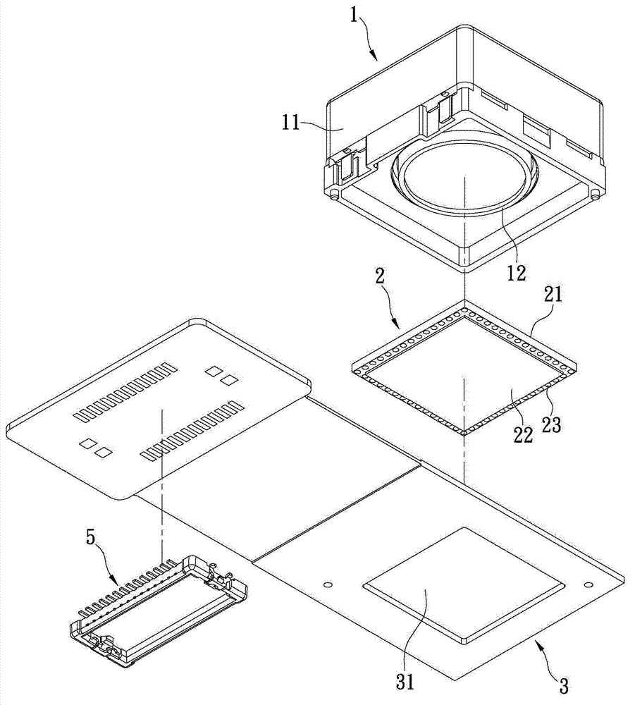
[0047] see Figure 1 to Figure 5 . The invention is an image module, figure 1 It is shown as a three-dimensional schematic diagram of the image module of the present invention. Such as figure 2 and image 3 As shown, the image module of the present invention includes a lens assembly 1 , an image sensing package 2 , a circuit board 3 , a passive element 4 , and a control element 5 .

[0048] The circuit board 3 defines an opening 31 . The lens assembly 1 is installed on the circuit board 3 and corresponds to the position of the opening 31 . The lens assembly 1 includes a casing 11 and a lens 12 , and the lens 12 is disposed in the casing 11 . The image sensing package 2 is disposed on the circuit board 3 , and the bottom of the image sensing package 2 is correspondingly placed in the opening 31 . The image sensing package 2 is located between the lens assembly 1 and the circuit board 3 .

[0049] In detail, the image sensing package 2 includes a glass substrate 21 and ...


PUM


Abstract

The invention discloses an image module and a manufacturing method thereof. The image module comprises a lens assembly, an image sensing package part and a circuit board. The circuit board is provided with an opening. The lens assembly is arranged on the circuit board and is arranged at the position corresponding to the opening. The image sensing package part is arranged on the circuit board, and the bottom of the image sensing package part is correspondingly inserted into the opening. The manufacturing method of the image module comprises the steps that the circuit board with the opening is provided and formed; a number of solder balls of an image sensing package part of a raw material are removed to form the image sensing package part whose solder balls are removed; the image sensing package part is corresponding to the opening; and by using a surface adhesion mode, the image sensing package part is fixedly connected with the circuit board, and the lens assembly is arranged on the circuit board.

Description

technical field [0001] The invention relates to a module and its manufacturing method, in particular to an image module and its manufacturing method. Background technique [0002] In today's era of advanced technology, most portable electronic products, such as mobile phones or tablet computers, are mostly equipped with image modules, and the development trend of portable electronic products is light, thin, short and small, so the configuration The image module also needs to be thinned correspondingly, so as to meet the current demand for thinning products. [0003] For this reason, see Figure 6A and Figure 6B , some industry once developed a package structure (the industry called Neo Pac package) which is mainly composed of a glass substrate 21' and an image sensor chip 22' packaged to form an image sensor package 2' of a raw material, By packaging the image sensing chip 22' on the bottom of the glass substrate 21', it can provide an excellent small package size. Howev...

Claims


Application Information

Patent Timeline
Patent Type & Authority Applications(China)
IPC IPC(8): H04N5/225H04N5/335H01L27/146
Inventor 赖孟修郑顺舟林昭琦
Owner BISON ELECTRONICS
Why Eureka
Try Eureka