Image module and manufacturing method thereof

A manufacturing method and image technology, applied in radiation control devices and other directions, to achieve the effect of reducing bad wear and tear and reducing the overall height

Inactive Publication Date: 2013-12-25
BISON ELECTRONICS
View PDF6 Cites 2 Cited by
  • Summary
  • Abstract
  • Description
  • Claims
  • Application Information

AI Technical Summary

Problems solved by technology

However, there are still defects: the image sensor 20 "and the lens module 10" are arranged on the same board surface, resulting in a high stacking height. Die Bond and Wire bond will produce a height of 50" for wiring and 60" for sealing

Method used


Image

  • Image module and manufacturing method thereof
  • Image module and manufacturing method thereof
  • Image module and manufacturing method thereof

Examples


Embodiment Construction

[0040] In order to have a further understanding of the purpose of the present invention, structure, feature, and function thereof, now cooperate embodiment to describe in detail as follows:

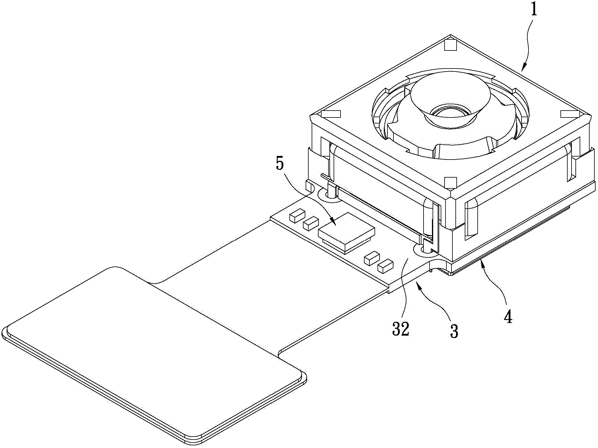
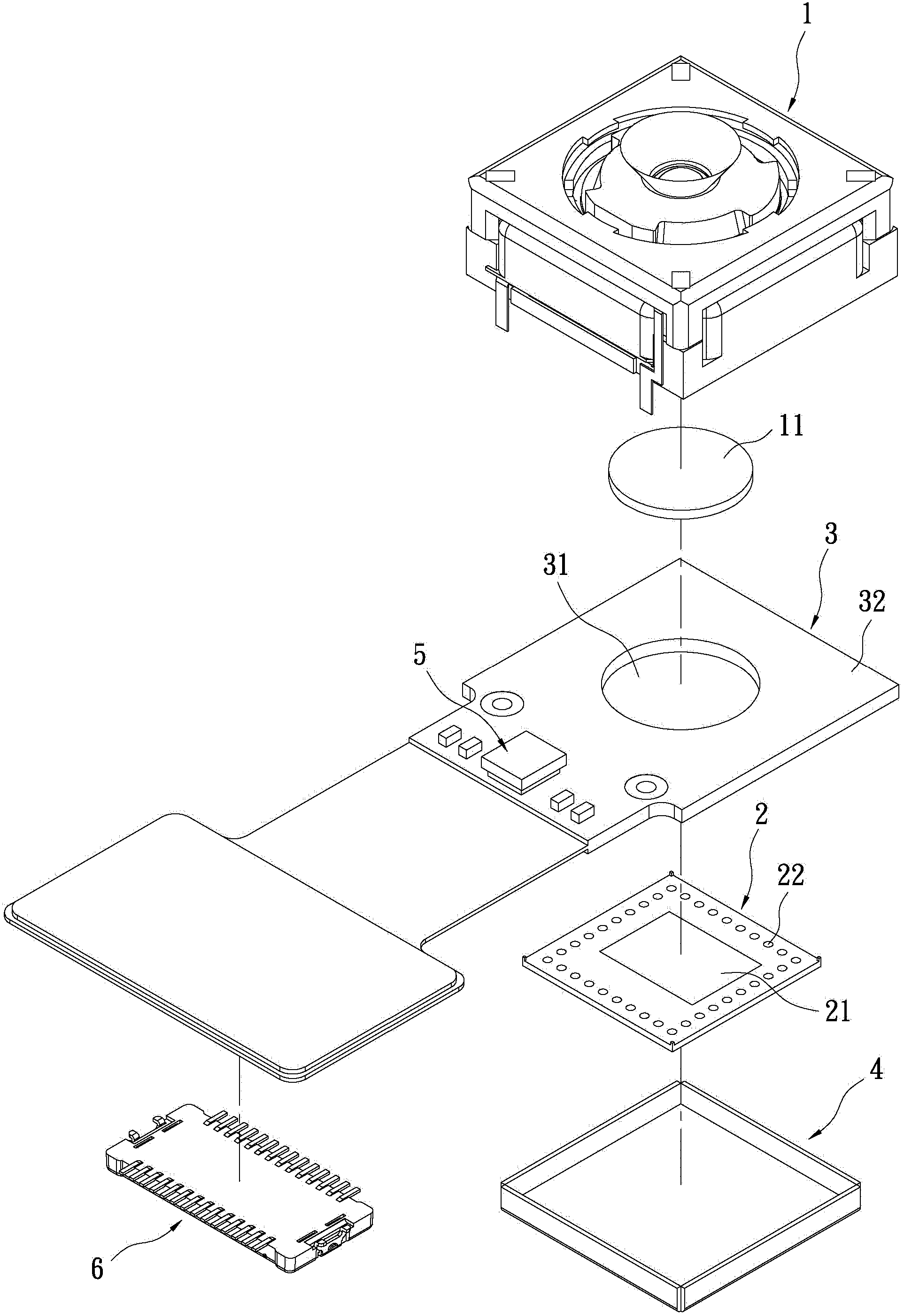
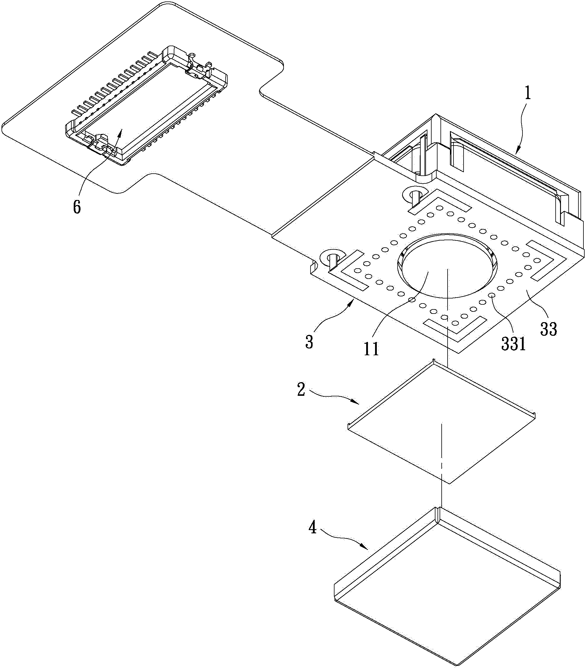
[0041] see figure 1 , and see Figure 2A and Figure 2B . The image module of the present invention includes a lens assembly 1 , an image sensing element 2 , a circuit board 3 , a packaging case 4 , a passive element 5 , and a control element 6 .

[0042] The circuit board 3 has an opening 31 , a first board surface 32 , and a second board surface 33 . The image sensing element 2 is disposed on the second plate surface 33 and corresponds to the opening 31. Specifically, the image sensing element 2 is an unpackaged sensing chip (Sensor Die) with a sensing region 21, the sensing region 21 corresponds to the opening 31 of the circuit board 3 .

[0043] The lens assembly 1 is mounted on the first board surface 32 and corresponds to the opening 31 . The lens assembly 1 further includes ...


PUM


Abstract

The invention discloses an image module and a manufacturing method thereof. The image module comprises a lens assembly, an image sensing component, an anisotropic conductive adhesive and a circuit board. The circuit board possesses a first plate surface and a second plate surface. The image sensing component is arranged on the second plate surface. The lens assembly is arranged on the first plate surface. The anisotropic conductive adhesive is arranged between the second plate surface of the circuit board and the image sensing component so that the image sensing component is electrically connected to the circuit board. The manufacturing method of the image module comprises the following steps that the anisotropic conductive adhesive is coated on the second plate surface; thermal compression bonding processing is performed on the image sensing component and the anisotropic conductive adhesive so that the image sensing component is fixedly connected and electrically connected with the second plate surface; the lens assembly is arranged on the first plate surface and the image sensing component is packaged.

Description

technical field [0001] The invention relates to a module and its manufacturing method, in particular to an image module and its manufacturing method. Background technique [0002] The development of modern electronic products is becoming more and more thin and miniaturized. At present, most of the image-related products are still produced in the traditional SMT (Surface-mount Technology) method, but the SMT process is limited by the sensing element ( Sensor Die) needs to be packaged with COB (Chip on Board) first before SMT can be carried out, so that the total height and cost of the image module cannot be reduced, which is not conducive to the demand for thinning, and the higher-level COB / FLIP CHIP process, although The height of the image module can be reduced, but its construction and maintenance costs are too high, and if it does not reach a certain scale of production, there will be no economic benefits. [0003] For this reason, see Figure 5 , there was an industry d...

Claims


Application Information

Patent Timeline
Patent Type & Authority Applications(China)
IPC IPC(8): H01L27/146
Inventor 赖孟修郑顺舟林昭琦
Owner BISON ELECTRONICS
Why Eureka
Try Eureka