Semiconductor packaging component with cooling fan and stacking structure thereof

A cooling fan and stack structure technology, applied in semiconductor devices, semiconductor/solid-state device components, electric solid-state devices, etc., can solve problems such as the use quality of electronic products that affect the cooling fan, noise generation, and thinning of the cooling fan.

Inactive Publication Date: 2013-04-10
AMTEK SEMICON
View PDF3 Cites 0 Cited by
  • Summary
  • Abstract
  • Description
  • Claims
  • Application Information

AI Technical Summary

Problems solved by technology

[0008] However, the formation of the extended portion 11a of the above-mentioned printed circuit board 11' will interfere with the airflow driven by the fan wheel 13' when it rotates. If the airflow is disturbed, noise will be generated, which will further affect the cooling fan installed. The quality of electronic products
At the same time, because the extension part 11a is extended outward, a predetermined distance needs to be maintained between the blade 132' and the control chip 110', which is not conducive to the reduction of the overall height of the existing cooling fan, and cannot meet the thinning requirements of electronic products. needs
[0009] Moreover, the aforementioned existing heat dissipation fan still needs to arrange the printed circuit board 11' between the hub 130' of the fan wheel 13' and the base 120' of the housing 12', resulting in the thickness of the printed circuit board 11' still affecting heat dissipation. The overall height of the fan, without further thinning the cooling fan

Method used


Image

  • Semiconductor packaging component with cooling fan and stacking structure thereof
  • Semiconductor packaging component with cooling fan and stacking structure thereof
  • Semiconductor packaging component with cooling fan and stacking structure thereof

Examples


no. 1 Embodiment

[0074] see Figure 2A to Figure 2E , is a cross-sectional view of the manufacturing method of the semiconductor package with cooling fan of the present invention.

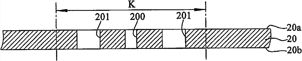
[0075] Such as Figure 2A As shown, first, a substrate 20 having a first surface 20a and a second surface 20b is provided, and the first surface 20a of the substrate 20 has a fan placement area K; The opening 200 and the ventilation hole 201. Such as Figure 2A' As shown, in this embodiment, the opening 200 is surrounded by four ventilation holes 201 . Of course, the present invention does not limit the number and shape of the ventilation holes, and there may be only two or more ventilation holes, and the ventilation holes may also be in a honeycomb shape.

[0076] Such as Figure 2B As shown, a plurality of electronic components 21 are arranged on the first surface 20a around the fan placement area K, and the electronic components 21 are electrically connected to the substrate 20; the electronic components 21...

no. 2 Embodiment

[0099] In another manufacturing method of a semiconductor package with a cooling fan of the present invention, as Figure 3A and Figure 3B As shown, electronic components 21 are disposed on the first surface 20a around the fan placement area K, including functional chips 21c, which are disposed on the substrate 20 and embedded in the encapsulant 22 after forming. In addition, in this preferred embodiment, heat dissipation pads 27 are formed on the first surface 20a and the second surface 20b of the substrate 20; The chip 21c is disposed on the thermal pad 27 on the first surface 20a of the substrate 20 . In addition, conductive connection elements 26' such as solder balls can also be connected to the heat dissipation pad 27 under the second surface 20b, so as to transmit heat energy to the bottom of the substrate 20 and / or communicate with other electrical devices through the conductive connection elements 26'. electrical connection.

no. 3 Embodiment

[0101] Such as Figure 4A to Figure 4C shown, for the continuation Figure 2E The present invention also provides a semiconductor package stack structure 3 with a heat dissipation fan, including: a semiconductor package 2 with a heat dissipation fan according to the present invention; a bottom electrical device 4, including a carrier 41 and located on the carrier The electronic component 43 on the component 41; and the conductive bonding material 31 such as a solder ball is arranged between the semiconductor package 2 and the bottom electrical device 4, and the substrate 20 of the semiconductor package 2 is connected to the conductive bonding material 31. material 31 , so that an air passage W is formed between the semiconductor package 2 and the bottom electrical device 4 , so that the fan unit 23 can dissipate the heat generated by the bottom electrical device 4 through the air passage W.

[0102] Such as Figure 4A As shown, the carrier 41 included in the aforementioned b...


PUM


Abstract

The invention discloses a semiconductor packaging component with a cooling fan and a manufacturing method and a stacking structure thereof. The semiconductor packaging component with the cooling fan comprises a substrate, an electronic element, a packaging rubber body and a fan unit, wherein the substrate is provided with a first surface and a second surface, the first surface is provided with a fan arrangement area, the fan arrangement area of the substrate is provided with an open hole and a ventilation hole penetrating through the substrate; the electronic element is arranged on the first surface and around the fan arrangement area and is electrically connected with the substrate; the packaging rubber body is formed on the electronic element and the first surface of the substrate and is provided with a packaging rubber body opening for the exposure of the fan arrangement area; and the fan unit is arranged in the packaging rubber body opening and is electrically connected with the substrate. Since the electronic element is arranged on the part of the substrate outside the fan arrangement area, when the fan unit operates normally, heat produced by the electronic element can be effectively dissipated and can be prevented from being damaged as a result of overheating, and the overall height of the fan unit can be reduced.

Description

technical field [0001] The invention relates to a semiconductor package and its manufacturing method, in particular to a semiconductor package with cooling fan and its manufacturing method. Background technique [0002] If the main board (Main Board or Mother Board) has a plurality of electronic components (Electronic Components) such as a central processing unit or graphics card and electrical circuits (Conductive Circuits) for electrically connecting the electronic components, The electronic components will generate heat when they function. If the generated heat is not removed from the electronic product equipped with the circuit board, the electronic components will fail due to overheating; Faster electronic products are more important, because the improvement of functions and processing speed means that the electronic components or electronic devices integrated on the circuit board need to be more or higher-level, and more or higher-level electronic components or electro...

Claims


Application Information

Patent Timeline
Patent Type & Authority Patents(China)
IPC IPC(8): H01L23/467H05K7/20F04D25/08
CPCH01L2924/0002H01L2924/15311H01L2224/48091H01L2224/48227
Inventor 曾祥伟
Owner AMTEK SEMICON
Why Eureka
Try Eureka