Multi-chip packaging body and packaging method

A multi-chip packaging and packaging method technology, which is applied in the fields of electric solid-state devices, semiconductor devices, semiconductor/solid-state device manufacturing, etc., can solve the problems of small number of chips, single function, and inability to meet the new needs of the electronic market, so as to save space. Effect

Inactive Publication Date: 2014-04-16
DIODES SHANGHAI +2
View PDF3 Cites 5 Cited by
  • Summary
  • Abstract
  • Description
  • Claims
  • Application Information

AI Technical Summary

Problems solved by technology

However, due to the small number of packaged chips in the traditional package, the functions that can be realized are very single, which cannot meet the new needs of customers in the electronic market.
Only a variety of different packages can be used to realize the corresponding single function, which leads to the inability to realize the miniaturization and portability of electronic terminal products

Method used


Image

  • Multi-chip packaging body and packaging method
  • Multi-chip packaging body and packaging method
  • Multi-chip packaging body and packaging method

Examples


Embodiment Construction

[0024] The specific implementation of the multi-chip package and its packaging method provided by the present invention will be described in detail below with reference to the accompanying drawings.

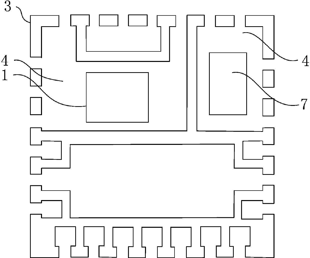
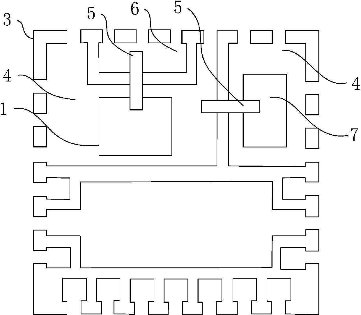
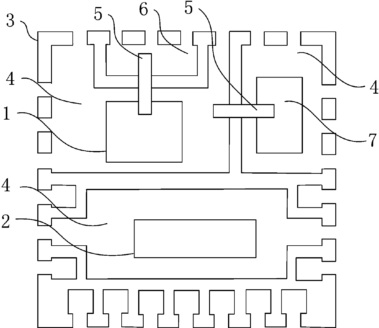
[0025] figure 1 Shown is the flow chart of the packaging method of the multi-chip package of the present invention, see figure 1 , the packaging method includes the following steps: step S10, using tin powder solder to weld the first functional chip on the chip base of the lead frame; step S11, using chip bonding wire to bond the first functional chip to the pins of the lead Connecting, the chip bonding wire is welded with the electrode of the first functional chip and the pin of the lead frame with tin powder solder; step S12, heating the lead frame for the first time to solidify the tin powder solder; step S13, welding the controller chip on the chip base of the lead frame with a welding adhesive; step S14, heating the lead frame for the second time to cure the welding adhesiv...


PUM


Abstract

The invention provides a multi-chip packaging body and a packaging method. The multi-chip packaging body comprises a first function chip and a controller chip. The first function chip and the controller chip are arranged on a chip base of a lead frame respectively. The first function chip is welded on the chip base through tin welding powder and is connected to a pin of the lead frame through a chip welding wire. The first function chip is connected with and transmits dynamic signals to the controller chip so that the controller chip can determine working state and give real-time protection. The multi-chip packaging body and the packaging method have the advantages that the functional chip and the controller chip are arranged on the same lead frame, horizontally achieving multi-chip packaging, saving internal space of electronic products and achieving downsizing and lightweight of electronic products. A plurality of chips integrated in the multi-chip package structure can achieve different functions respectively, so that multi-function and high integration of electronic products are achieved. Besides, the chip is connected with the pin through the chip welding wire in an electrical mode, which is more suitable for high-power devices.

Description

technical field [0001] The invention relates to the technical field of semiconductor packaging, in particular to a multi-chip package and a packaging method thereof. Background technique [0002] With the development of semiconductor technology, integrated circuits have become multi-functional and highly integrated, requiring the package to be able to realize multiple different functions at the same time. However, due to the small number of chips packaged in the traditional package, the functions that can be realized are very single, and cannot meet the new needs of customers in the electronic market. Only a variety of different packages can be used to realize the corresponding single function respectively, resulting in the inability to realize the miniaturization and portability of electronic terminal products. Contents of the invention [0003] The technical problem to be solved by the present invention is to provide a multi-chip package and its packaging method, which ...

Claims


Application Information

Patent Timeline
Patent Type & Authority Applications(China)
IPC IPC(8): H01L25/00H01L23/31H01L23/495H01L21/50H01L21/60
CPCH01L2224/48137H01L2224/49171H01L2224/48247H01L2224/4903H01L2224/73221
Inventor 许文耀董美丹
Owner DIODES SHANGHAI
Why Eureka
Try Eureka