Driving method and driving circuit of display panel

A technology of display panel and driving method, applied in static indicators, instruments, etc., can solve the problems of poor image quality, large equivalent resistance and capacitive load, large difference in center uniformity, etc., to compensate for the difference in charging effect, The effect of uniform brightness and improved uniformity

Inactive Publication Date: 2014-04-23
TCL CHINA STAR OPTOELECTRONICS TECH CO LTD
View PDF5 Cites 39 Cited by
  • Summary
  • Abstract
  • Description
  • Claims
  • Application Information

AI Technical Summary

Problems solved by technology

[0002] At present, the resolution and size of liquid crystal displays are getting larger and larger, and the equivalent resistance and capacitance load on the equivalent transmission path corresponding to the panel with thin film transistor (TFT) as the main driving method is getting larger and larger, such as figure 1 As shown, the data signal gate output by the data-driven integrated circuit (Data IC) will have a waveform when the first scan signal arrives (such as figure 2 shown), and the data signal at the position of the nth scanning line will be mutated as image 3 The waveform shown, this kind of variation is usually called RC delay in the industry, so for the same data line, there will be different charging effects at different vertical positions, and in severe cases, it will cause large differences in the uniformity of the upper, lower and center. Big, poor video quality

Method used


Image

  • Driving method and driving circuit of display panel
  • Driving method and driving circuit of display panel
  • Driving method and driving circuit of display panel

Examples


Embodiment 1

[0039] Such as Figure 4 As shown, this implementation mode discloses a driving method of a display panel, including steps:

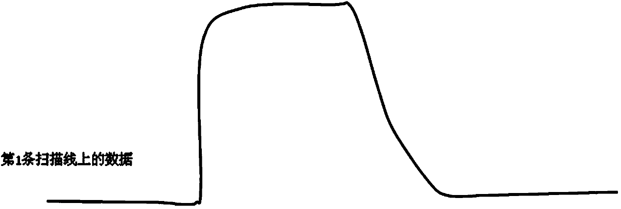
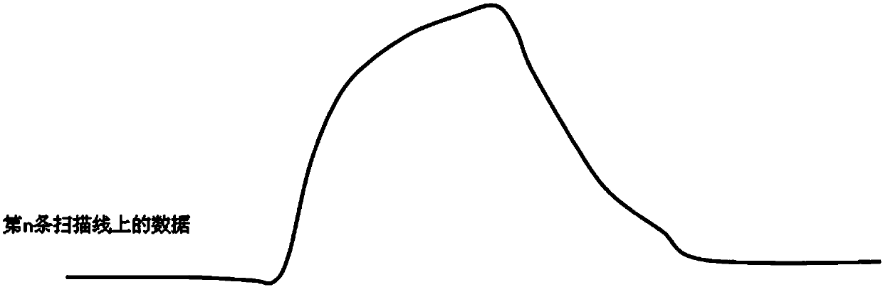
[0040] S1. Setting the driving time T of the scanning line of the first row;

[0041] S2. Calculate the incremental value ΔT of the driving time of each scanning line according to the vertical blanking time T1 of two adjacent frames and the total number N of scanning lines;

[0042] S3. Drive the scan lines of the display panel row by row; first drive the scan lines of the previous row;

[0043] S4, and then drive the next row of scanning lines; within the display time of one frame, the driving time of the next row of scanning lines is greater than the driving time of the previous row of scanning lines, and the difference between the driving times of two adjacent scanning lines is △T ;

[0044] Suppose the driving time of the first scanning line is T, the total number of scanning lines is N, the vertical blanking time of two adjacent frames is T1, an...

Embodiment 2

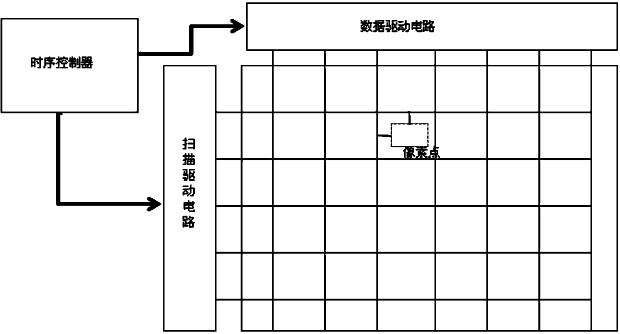
[0050] Such as Figure 6 As shown, the present invention discloses a driving method and a driving circuit of a display panel. The driving circuit includes a scanning line 30 and a scanning line driving module connected to the scanning line 30 . The timing module 10 includes a timing controller 12 and a storage unit 11, and the timing controller 12 includes a driving unit 13 that increases the driving time of the scanning lines row by row;

[0051] The driving unit 13 reads the difference between the driving times of two adjacent scanning lines from the storage unit 11 , generates a driving signal and sends it to the scanning line driving circuit 20 .

[0052] Suppose the driving time of the first scanning line is T, the total number of scanning lines is N, the vertical blanking time of two adjacent frames is T1, and the sum of driving time of all scanning lines is Tm, then the difference between Tm and T×N is less than or equal to T1.

[0053] Of course, the difference betw...


PUM


Abstract

The invention discloses a driving method and driving circuit of a display panel. The driving method of the display panel comprises the following steps: driving scanning lines of the display panel row by row; within the time of displaying a frame of an image, the driving time of at least one scanning line being greater than the driving time of a first scanning line; and within a period of one frame, the total driving time of all the scanning lines not exceeding a displaying time of a single frame. According to the invention, the problem of uneven brightness of the driving panel is improved, the product uniformity is improved, and the taste is improved.

Description

technical field [0001] The present invention relates to the field of liquid crystal display, and more specifically, relates to a driving method and a driving circuit of a display panel. Background technique [0002] At present, the resolution and size of liquid crystal displays are getting larger and larger, and the equivalent resistance and capacitance load on the equivalent transmission path corresponding to the panel with thin film transistor (TFT) as the main driving method is getting larger and larger, such as figure 1 As shown, the data signal gate output by the data-driven integrated circuit (Data IC) will have a waveform when the first scan signal arrives (such as figure 2 shown), and the data signal at the position of the nth scanning line will be mutated as image 3 The waveform shown, this kind of variation is usually called RC delay in the industry, so for the same data line, there will be different charging effects at different vertical positions, and in sever...

Claims


Application Information

Patent Timeline
Patent Type & Authority Applications(China)
IPC IPC(8): G09G3/36G02F1/133
CPCG09G3/3611G09G2310/0202G09G3/3648G09G2310/08G09G2320/0223
Inventor 谭小平
Owner TCL CHINA STAR OPTOELECTRONICS TECH CO LTD
Why Eureka
Try Eureka