FPGA testing device and method

A test configuration and self-test technology, which is applied in the field of FPGA test devices, can solve the problems of optimization effect influence, test cost increase, test efficiency impact, etc., to achieve the effect of improving test efficiency, reducing the number of times, and reducing test cost

Active Publication Date: 2014-05-14
INST OF ELECTRONICS CHINESE ACAD OF SCI
View PDF5 Cites 16 Cited by
  • Summary
  • Abstract
  • Description
  • Claims
  • Application Information

AI Technical Summary

Problems solved by technology

This type of method is more effective for FPGAs with a relatively regular structure, but with the increasing complexity of the FPGA array, the optimization effect brought by this type of method is greatly affected
[0006] The applicant found that the existing technology has the following technical defects: the overhead caused by the loading test configuration is very large, which affects the test efficiency and increases the test cost

Method used


Image

  • FPGA testing device and method
  • FPGA testing device and method
  • FPGA testing device and method

Examples


Embodiment Construction

[0023] In order to make the object, technical solution and advantages of the present invention clearer, the present invention will be described in further detail below in conjunction with specific embodiments and with reference to the accompanying drawings.

[0024] The device and method for testing FPGA of the present invention convert the test configuration in the FPGA configuration memory into another group of effective test configurations by utilizing the feedback and superposition device in the data generator and the address generator, so as to reduce the serial number from the outside of the chip. The number of times to load test configurations can be increased to improve test efficiency and reduce test costs.

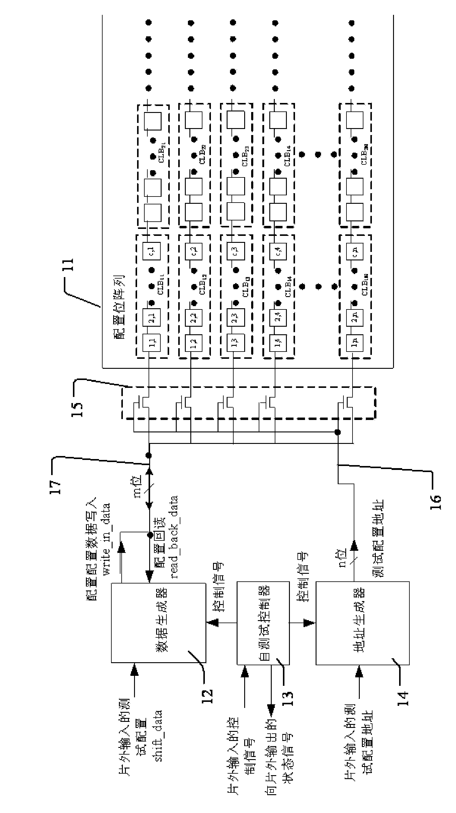
[0025] In an exemplary embodiment of the present invention, a device for testing FPGA is provided. Such as figure 1 As shown, the device for testing FPGA includes: a data generator 12 , an address generator 14 and a self-test controller 13 . Wherein, the self-t...


PUM


Abstract

The invention provides a FPGA testing device and method. The FPGA testing device is disposed in a FPGA chip and comprises a self-testing controller, an address generator, and a data generator. The self-testing controller is used for generating an address generating signal and backward read enabling signal according to a preset time sequence. The address generator is used for generating addresses containing a tested FPGA configuration array under the driving of the address generating signal, and enabling the FPGA configuration array corresponding to the addresses in a corresponding read-write state. The data generator is used for firstly reading configuration data from the FPGA configuration array and converting the configuration data into a set of new testing configuration data according to each address provided by the address generator under the effect of the backward read enabling signal, and then rewriting the newly-generated testing configuration data in the address of the FPGA configuration array. The FPGA testing device and method decrease the times of externally loading testing configuration in series of a chip, increase testing efficiency, and reduce testing cost.

Description

technical field [0001] The present invention relates to field programmable gate array (Field programmable gate array, FPGA for short) design field, particularly relate to a kind of device and method for testing FPGA. Background technique [0002] The generation test of FPGA is generally composed of multiple test sessions (test sessions). A test session FPGA test can be roughly divided into three steps: 1. Loading test configuration; 2. Loading stimulus; 3. Observing test response. The purpose of test configuration loading is to configure it into a specific circuit structure to facilitate testing. The test configuration code is a string of binary codes, the length of which can reach tens of millions to hundreds of millions of bits, and is serially downloaded to the configuration bit array of the FPGA to complete a test configuration load. Subsequently, a test stimulus is applied to obtain a test response. By comparing the obtained test response with the expected test respon...

Claims


Application Information

Patent Timeline
Patent Type & Authority Applications(China)
IPC IPC(8): G01R31/317
Inventor 王飞杨海钢
Owner INST OF ELECTRONICS CHINESE ACAD OF SCI
Why Eureka
Try Eureka