Light-emitting display back panel, organic light emitting displayer and manufacturing method of light-emitting display back panel and organic light emitting displayer

A light-emitting display device and a light-emitting display technology, which are applied in the manufacture of semiconductor/solid-state devices, electric solid-state devices, semiconductor devices, etc., can solve the problems of affecting the display effect, wear and deformation of the contact layer 2, and reducing the stability and reliability of organic light-emitting displays, etc. problem, to achieve the effect of improving stability and reliability

Active Publication Date: 2014-05-14
HISENSE VISUAL TECH CO LTD
View PDF6 Cites 30 Cited by
  • Summary
  • Abstract
  • Description
  • Claims
  • Application Information

AI Technical Summary

Problems solved by technology

Depend on Figure 1A and Figure 1B It can be seen that since the support 1 is a structure with a narrow top and a wide bottom, the contact layer 2 and the electrode layer 3 are a continuous whole. However, the contact layer 2 is in contact with the package substrate. Wear and deformation. At this time, the con...

Method used


Image

  • Light-emitting display back panel, organic light emitting displayer and manufacturing method of light-emitting display back panel and organic light emitting displayer
  • Light-emitting display back panel, organic light emitting displayer and manufacturing method of light-emitting display back panel and organic light emitting displayer
  • Light-emitting display back panel, organic light emitting displayer and manufacturing method of light-emitting display back panel and organic light emitting displayer

Examples


Embodiment Construction

[0036] The following will clearly and completely describe the technical solutions in the embodiments of the present invention in conjunction with the accompanying drawings in the embodiments of the present invention. Obviously, the described embodiments are only some of the embodiments of the present invention, not all of them. Based on the embodiments of the present invention, all other embodiments obtained by persons of ordinary skill in the art without making creative efforts belong to the protection scope of the present invention.

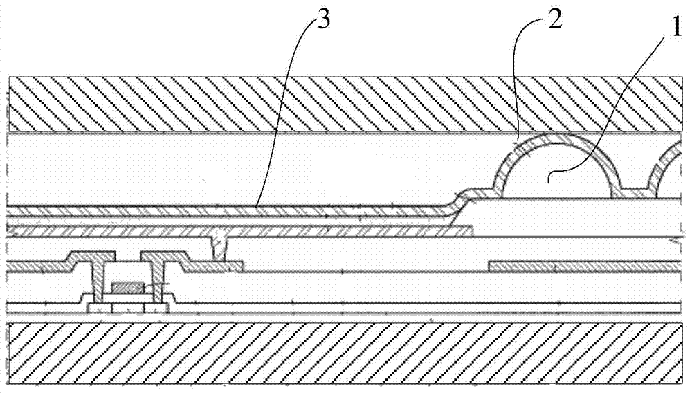
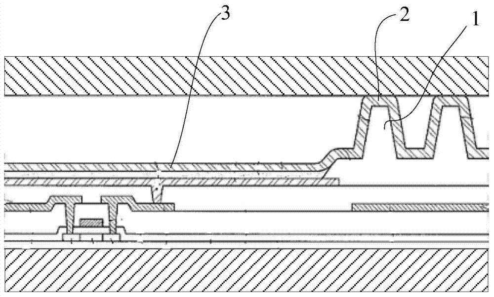
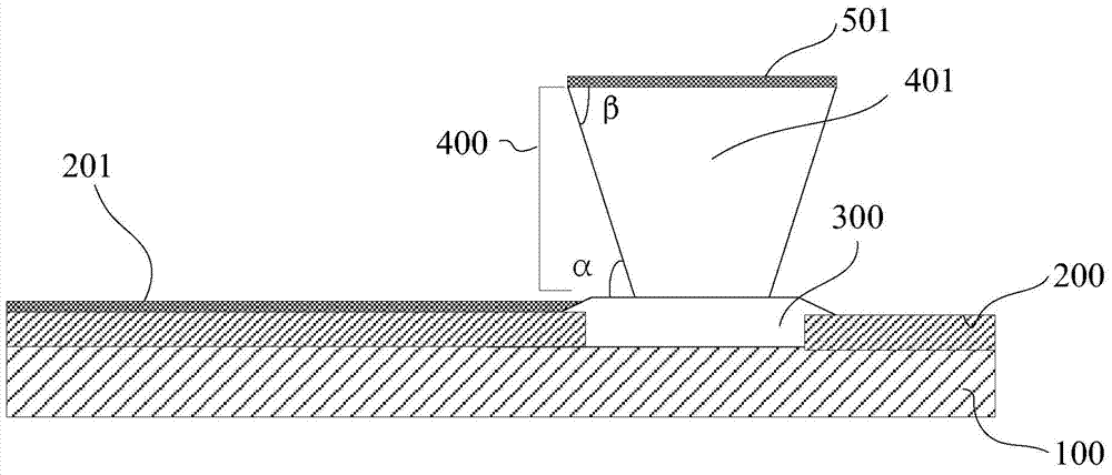
[0037] An embodiment of the present invention provides a light-emitting display backplane, such as Figure 2AAs shown, it includes several organic light emitting display devices 200 formed on the array substrate 100, and a pixel definition layer 300 arranged between adjacent organic light emitting display devices, and also includes a support 400 formed on the pixel definition layer 300 , wherein the support 400 includes a support part 401, the ...


PUM


Abstract

The invention discloses a light-emitting display back panel, an organic light emitting displayer and a manufacturing method of the light-emitting display back panel and the organic light emitting displayer. The light-emitting display back panel comprises a plurality of organic light emitting displayers formed on an array substrate and pixel definition layers between adjacent organic light emitting displayers. The light-emitting display back panel further comprises a plurality of supporting objects which are formed on the pixel definition layers and used for supporting packaging substrates arranged opposite to the light-emitting display back panel. Each supporting object comprises a supporting part, the cross sections of the supporting parts in the direction perpendicular to a plane where the array substrate is located are in inverted trapezoidal shapes which are trapezoids, the trapezoids are characterized in that the lengths of the upper bottoms of the inverted trapezoidal shapes are larger than the lengths of the lower bottoms of the inverted trapezoidal shapes, and included angles between the lower bottoms and the slant edges are obtuse angles. According to the light-emitting display back panel, the organic light emitting displayer and the manufacturing method, a contact layer and an electrode layer are of a discrete structure, the electrode layer cannot be influenced by deformation when the contact layer is deformed, and the stability and the reliability of the organic light emitting displayer are improved.

Description

technical field [0001] The invention relates to the field of display manufacturing, in particular to a light-emitting display backplane, an organic light-emitting display and a manufacturing method thereof. Background technique [0002] Organic Light Emitting Diode (OLED), due to its characteristics of self-luminescence, fast response, and wide viewing angle, OLED-based organic light-emitting displays have become mainstream products in the display field. [0003] The OLED-based organic light-emitting display includes a light-emitting display backplane and a packaging substrate. There is a gap of a certain thickness between the light-emitting display backplane and the packaging substrate. In order to cause deformation, a support for supporting the packaging substrate disposed opposite to the light-emitting display backplane is generally arranged on the light-emitting display backplane. [0004] Figure 1A and Figure 1B It is a schematic diagram of the structure of an exist...

Claims


Application Information

Patent Timeline
IPC IPC(8): H01L27/32H01L51/52H01L51/56
CPCH10K59/122H10K50/841H10K50/8428
Inventor 路林曹建伟
Owner HISENSE VISUAL TECH CO LTD
Why Eureka
Try Eureka