Identification structure in exposure process of high-density interconnection circuit board

A high-density interconnection and identification structure technology, which is applied in the field of high-density interconnection circuit board exposure technology, can solve the problems that product boards cannot be effectively traced, product boards have no identification, and cannot be found.

Inactive Publication Date: 2014-05-28
TIANJIN PRINTRONICS CIRCUIT CORP
View PDF0 Cites 2 Cited by
  • Summary
  • Abstract
  • Description
  • Claims
  • Application Information

AI Technical Summary

Problems solved by technology

[0003] After the above operation process is completed, the product board enters the next process for processing. However, in the existing process, it is impossible to find out which operator or which exposure machine completed the film exposure. This is mainly because there is no one on the product board. Effective identification, that is to say, once a problem occurs, the product board cannot be effectively traced

Method used


Image

  • Identification structure in exposure process of high-density interconnection circuit board
  • Identification structure in exposure process of high-density interconnection circuit board
  • Identification structure in exposure process of high-density interconnection circuit board

Examples


Embodiment Construction

[0013] Below in conjunction with the examples, the present invention is further described, the following examples are illustrative, not limiting, and the protection scope of the present invention cannot be limited by the following examples.

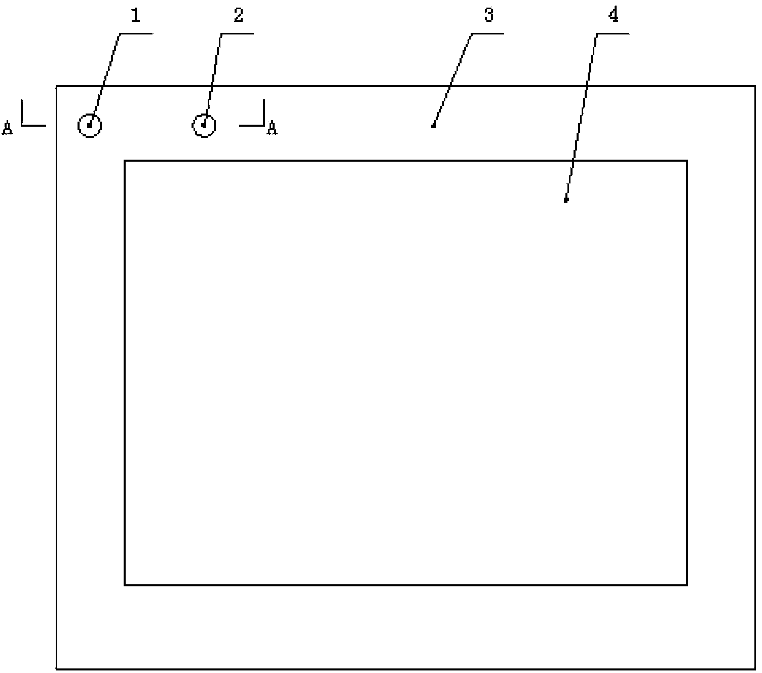
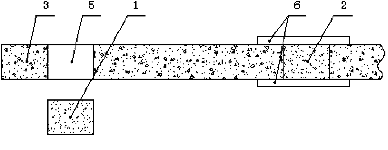
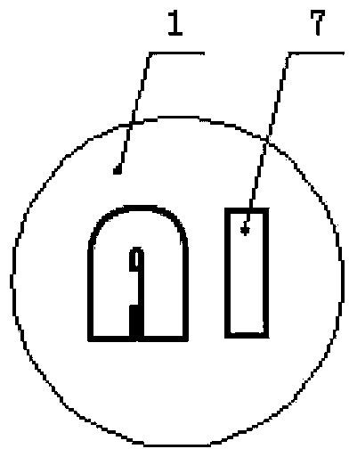
[0014] A recognition structure in a high-density interconnect circuit board exposure process, such as Figure 1~3 Shown, comprise film 3, be provided with figure area 4 on film, it is characterized in that: at least one through hole 5 is made on the film outside figure area, each through hole is embedded with a film that matches with through hole Blocks 1 and 2, each film block is connected to the film through a transparent adhesive tape 6, and an identification mark 7 is set on the film block.

[0015] In this embodiment, the film block is made of the same material as the film and has the same shape and size as the through hole made on the film. There are two film blocks, namely the operator identification film block 1 and the processing...


PUM


Abstract

The invention relates to an identification structure in an exposure structure of a high-density interconnection circuit board. The identification structure includes a film. A graphic area is arranged on the film. At least one through hole is manufactured in the film at the outer side of the graphic area. A film piece which cooperates with the through hole is embedded in each through hole. Each film piece is connected with the film through a scotch tape. Identification symbols are arranged on the film pieces. In the identification structure in the exposure process of the high-density interconnection circuit board, at least one through hole is manufactured in the film at the outer side of the graphic area and a film piece with an identification symbol is embedded in each through hole; when exposure is performed, the identification symbols on the film pieces are also transferred on a product board; and after an acid etching process, the product board is provided with the identification symbols which can show operators and manufacturing devices and thus during post processing, once problems occur, past manufacturing conditions can be traced well and significantly conveniently.

Description

technical field [0001] The invention belongs to the technical field of high-density interconnect circuit board exposure technology, in particular to an identification structure in the high-density interconnect circuit board exposure process. Background technique [0002] The circuit board uses insulating material as the base layer, and the copper foil wire layer and various electronic components are laid on the base layer. The circuit board has been widely used in all aspects of people's daily work and life. During the processing of the circuit board, the graphics on the film need to be transferred. The specific operation process is: first, the exposure of the film 3 is carried out, so that the graphics in the graphics area 4 on the film are transferred to the product board, and then the product board is acid-etched. The transfer of the graphics is done after processing. [0003] After the above operation process is completed, the product board enters the next process for p...

Claims


Application Information

Patent Timeline
Patent Type & Authority Applications(China)
IPC IPC(8): H05K3/06
Inventor 王彦博
Owner TIANJIN PRINTRONICS CIRCUIT CORP
Why Eureka
Try Eureka