Wafer cleaning equipment-based product tracking method and system

A technology for product tracking and cleaning equipment, which is applied in the direction of electrical components, semiconductor/solid-state device manufacturing, circuits, etc., and can solve problems such as inability to process products, record and query the operation process and status of wafer products, and inability to track wafer products , to achieve the effect of improving product yield

Inactive Publication Date: 2014-06-11
CSMC TECH FAB2 CO LTD
View PDF4 Cites 4 Cited by
  • Summary
  • Abstract
  • Description
  • Claims
  • Application Information

AI Technical Summary

Problems solved by technology

[0005] In the prior art, the wafer cleaning equipment is generally equipped with multiple ports, and the wafer products are placed in the ports for exhaust gas treatment. During the processing process, the operation process and status of the wafer products cannot be recorded and queried. If there is an abnormality in a certain step of the process or equipment, Unable to track wafer products, and thus unable to process problematic products

Method used


Image

  • Wafer cleaning equipment-based product tracking method and system
  • Wafer cleaning equipment-based product tracking method and system
  • Wafer cleaning equipment-based product tracking method and system

Examples


Embodiment Construction

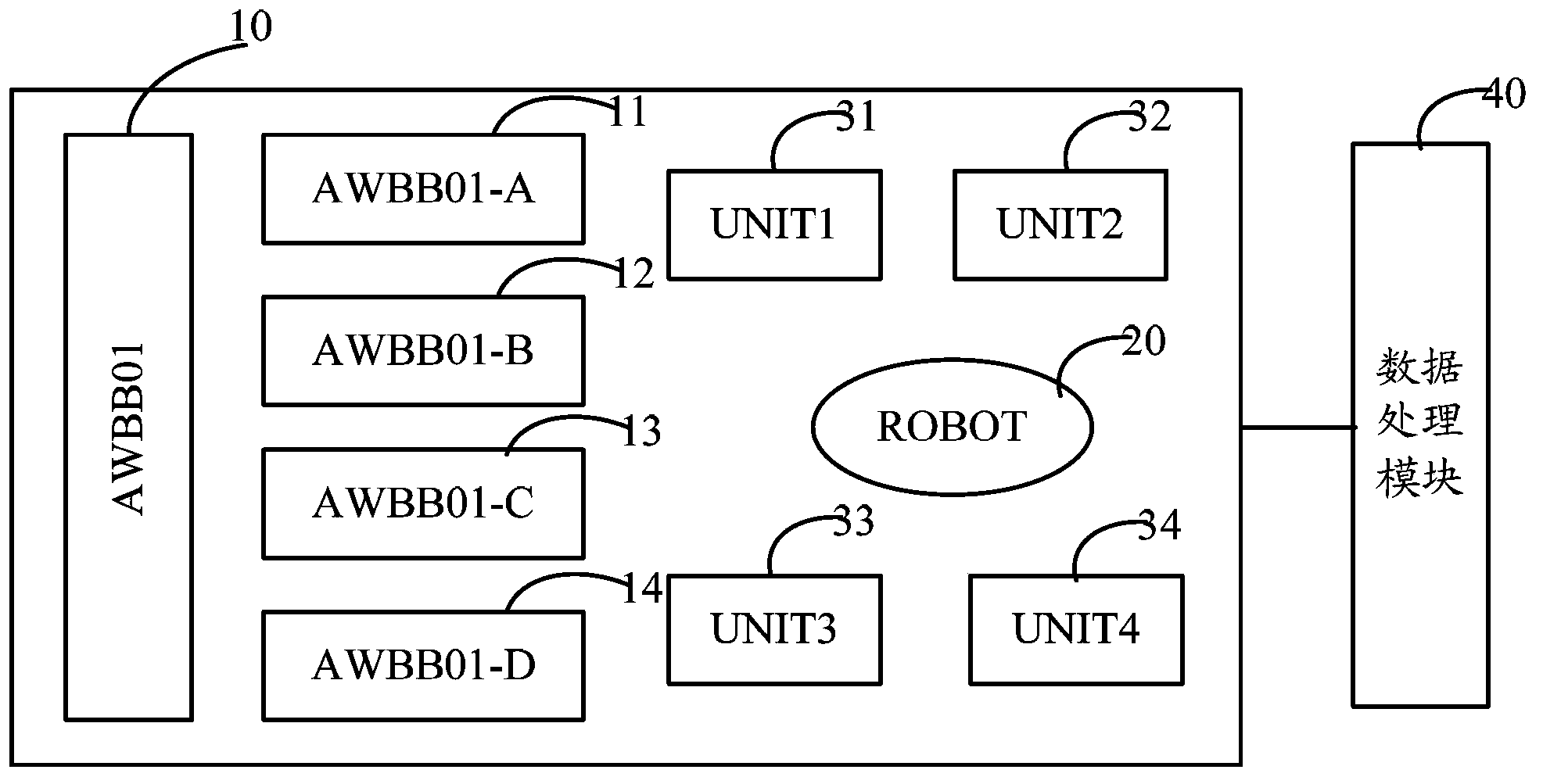
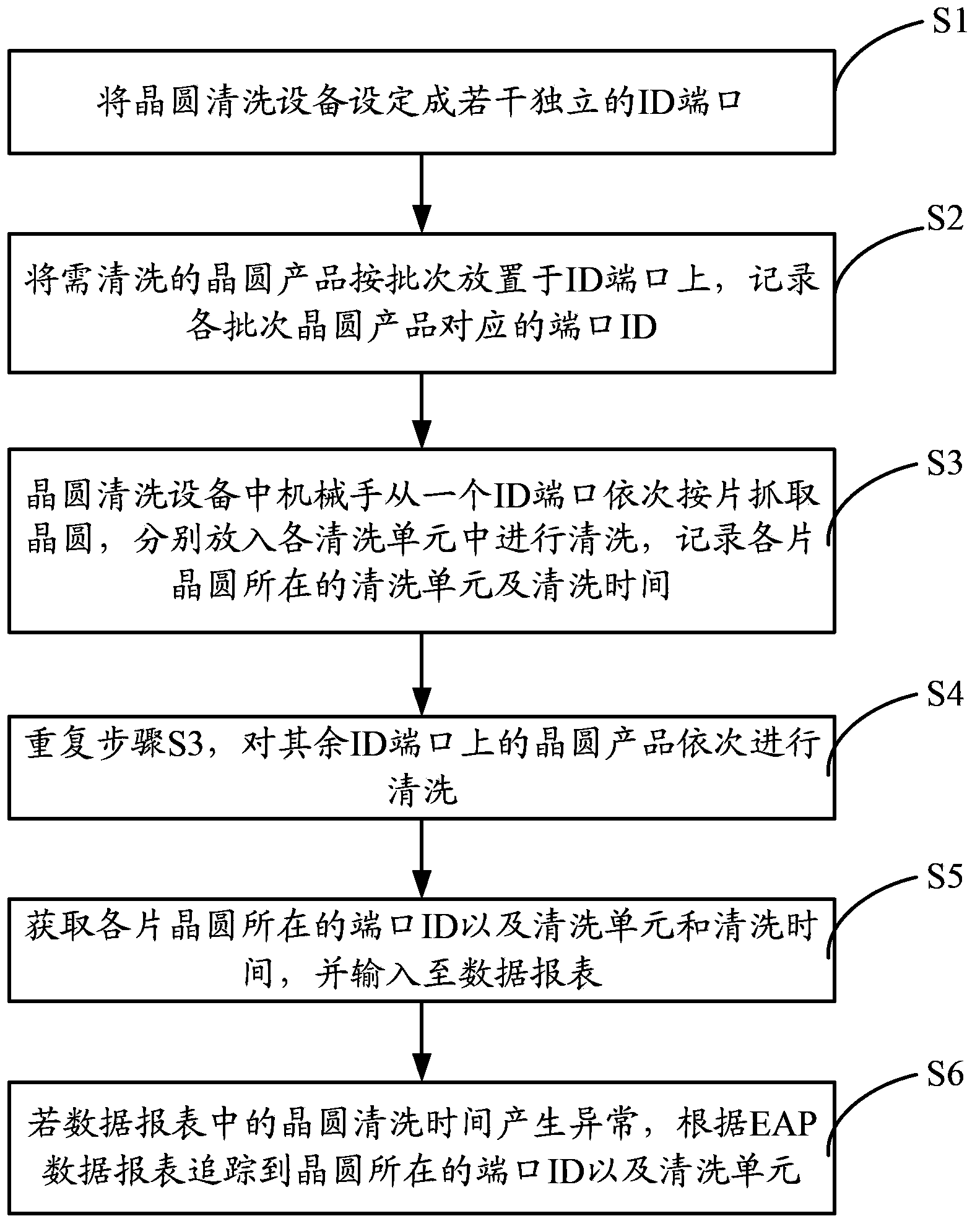
[0038] The invention discloses a product tracking method based on wafer cleaning equipment. The tracking method specifically includes:

[0039] S1. Set the wafer cleaning equipment to several independent ID ports;

[0040] S2. Place the wafer products to be cleaned on the ID port in batches, and record the port ID corresponding to each batch of wafer products;

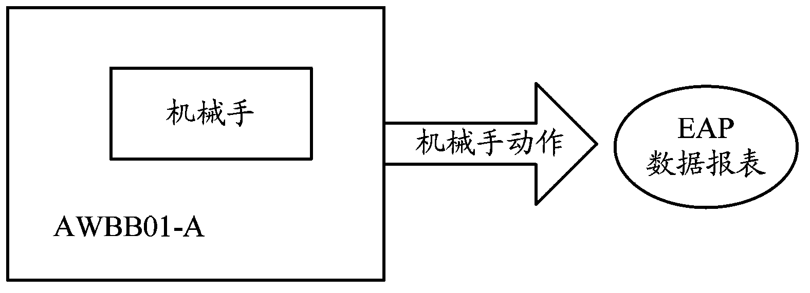
[0041] S3. The robotic arm in the wafer cleaning equipment sequentially grabs the wafers from an ID port, puts them into each cleaning unit for cleaning, and records the cleaning unit where each wafer is located and the cleaning time;

[0042] S4. Repeat step S3 to sequentially clean the wafer products on the remaining ID ports;

[0043] S5, obtain the port ID where each wafer is located, the cleaning unit and the cleaning time, and input them into the data report;

[0044] S6. If the wafer cleaning time in the data report is abnormal, track the port ID and cleaning unit where the wafer is located according to the da...


PUM


Abstract

The invention discloses a wafer cleaning equipment-based product tracking method and system. The method comprises the steps that: wafer cleaning equipment is set into a plurality of independent ID ports; wafer products that need to be cleaned are placed by batch at the ID ports; a mechanical arm of the wafer cleaning equipment grabs the wafers by sheet successively from one ID port and the wafers are respectively placed into all cleaning units for cleaning; the wafer products at the rest of ID ports are successively cleaned; port IDs where all wafers are located as well as cleaning units and cleaning times are obtained and the information is inputted into a data report; and if the wafer cleaning time in the data report is abnormal, the port IDs where the wafers are located at and the cleaning units are tracked according to the data report. According to the invention, the machine is set into independent ID ports and the process as well as the state of the product of each ID port is recorded in real time. Therefore, when the process is abnormal or the equipment works abnormally, inquiring can be carried out timely and accurately and the abnormal product can be tracked, thereby improving the yield.

Description

technical field [0001] The present invention relates to the technical field of semiconductor surface treatment, in particular to a method and system for product tracking based on wafer cleaning equipment. Background technique [0002] Wafer cleaning technology is extremely important to the electronics industry, especially to the semiconductor industry. In semiconductor devices and integrated circuits, cleaning is involved in almost every process, and the higher the integration of the integrated circuit, the more manufacturing processes and the more cleaning processes required. In many cleaning processes, as long as one process fails to meet the requirements, all previous efforts will be abandoned, which will lead to the scrapping of the whole batch of chips or the poor process. [0003] Wafer cleaning mainly removes various impurities adsorbed on the surface of the wafer, such as particles, organic matter, inorganic metal ions, etc., so that the surface purity of the wafer ...

Claims


Application Information

Patent Timeline
Patent Type & Authority Applications(China)
IPC IPC(8): H01L21/02H01L21/67
CPCH01L21/02041H01L21/67023H01L21/67253
Inventor 栾广庆
Owner CSMC TECH FAB2 CO LTD
Why Eureka
Try Eureka