FPGA automatic logic loading device and method

An automatic loading and logic technology, applied in the direction of program control device, program loading/starting, etc., can solve the problems of high cost and poor reliability of loading logic

Inactive Publication Date: 2014-06-18
LUOYANG INST OF ELECTRO OPTICAL EQUIP OF AVIC
View PDF4 Cites 13 Cited by
  • Summary
  • Abstract
  • Description
  • Claims
  • Application Information

AI Technical Summary

Problems solved by technology

[0004] The purpose of this invention is to provide a kind of device that FPGA automatically loads logic, to solve the problem that the cost of existing FPGA load logic is high or poor reliability

Method used


Image

  • FPGA automatic logic loading device and method
  • FPGA automatic logic loading device and method

Examples


Embodiment Construction

[0015] The present invention will be described in further detail below in conjunction with the accompanying drawings.

[0016] Device embodiment of the present invention:

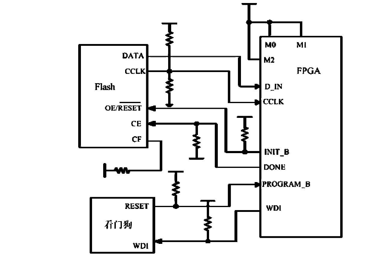
[0017] figure 1 Schematic diagram of the device for automatically loading logic for FPGA. The FPGA automatic loading logic device includes an FPGA chip and a FLASH memory that are connected correspondingly through signal lines, and also includes a watchdog chip. The reset output signal RESET terminal of the watchdog chip is connected to the start loading signal PROGRAM_B terminal of the FPGA chip. The dog feeding signal WDI end of the dog chip is connected to the corresponding WDI signal end of the FPGA chip.

[0018] In this example, the FPGA is configured as Slave Serial, assuming that the FPGA loading mode is slave serial, and the CF signal is not used. The selection of the watchdog chip must satisfy that its timeout time is less than the sum of the time required for the FPGA to load the logic and fee...


PUM


Abstract

The invention relates to an FPGA automatic logic loading device and method. The FPGA automatic logic loading device comprises an FPGA chip and a FLASH memorizer which are correspondingly connected through a signal line, and further comprises a watchdog chip, wherein a reset output signal RESET end of the watchdog chip is connected with a starting loading signal PROGRM_B end, a dog-feeding signal WDI end of the watchdog chip is connected with a corresponding WDI signal end of the FPGA chip. The watchdog chip is connected with an FPGA automatic logic loading logic circuit, when FPGA logic loading is unsuccessful or a product operates abnormally or dog feeding is not normal, a RESET signal outputs low pulse, an FPGA logic loading timing sequence is started till the logic loading is successful and the product operates abnormally, the FPGA operation situation monitoring and automatic logic loading can be achieved without other CPU or DSP and control chips, the device cost is reduced, and the control reliability is improved.

Description

technical field [0001] The invention relates to a device and a method for automatically loading logic on an FPGA during product operation. Background technique [0002] In current circuit design, with the continuous improvement of FPGA (Field Programmable Gate Array, field programmable gate array) chip integration, more and more designs adopt the architecture of FPGA plus peripheral circuits, and realize it by utilizing the rich logic resources inside FPGA. own function. The design architecture with FPGA as the core puts forward higher requirements on the reliability of FPGA. Nowadays, complex FPGA chips and logic need to be stored in FLASH and other memories first. When the system is powered on, the data is loaded from FLASH to FPGA through a specific interface for operation. [0003] In order to realize the control of FPGA loading logic, it is common practice to monitor the operation of FPGA through controllers such as CPU or DSP chip in the circuit, and control whether ...

Claims


Application Information

Patent Timeline
Patent Type & Authority Applications(China)
IPC IPC(8): G06F9/445
Inventor 陈超郭晓光孙艺
Owner LUOYANG INST OF ELECTRO OPTICAL EQUIP OF AVIC
Why Eureka
Try Eureka