

Semiconductor treatment technology and semiconductor device preparation method
一种处理工艺、半导体的技术,应用在半导体器件、半导体/固态器件制造、晶体管等方向,能够解决影响嵌入硅锗器件性能等问题
Inactive Publication Date: 2014-06-18
SHANGHAI HUALI MICROELECTRONICS CORP
View PDF6 Cites 7 Cited by
- Summary
- Abstract
- Description
- Claims
- Application Information
AI Technical Summary
Problems solved by technology
[0010] However, in actual operation, the formed e-SiGe will have dislocation defects, such as figure 2 Shown in the oval box ( figure 2 The middle black part represents silicon germanium material), which affects the performance of embedded silicon germanium devices
Method used
View moreImage
Smart ImageViewing Examples

Examples
preparation example Construction
[0054] Further, the above-mentioned semiconductor processing technology can be applied to a method for preparing a semiconductor device, and the method for preparing a semiconductor device includes:
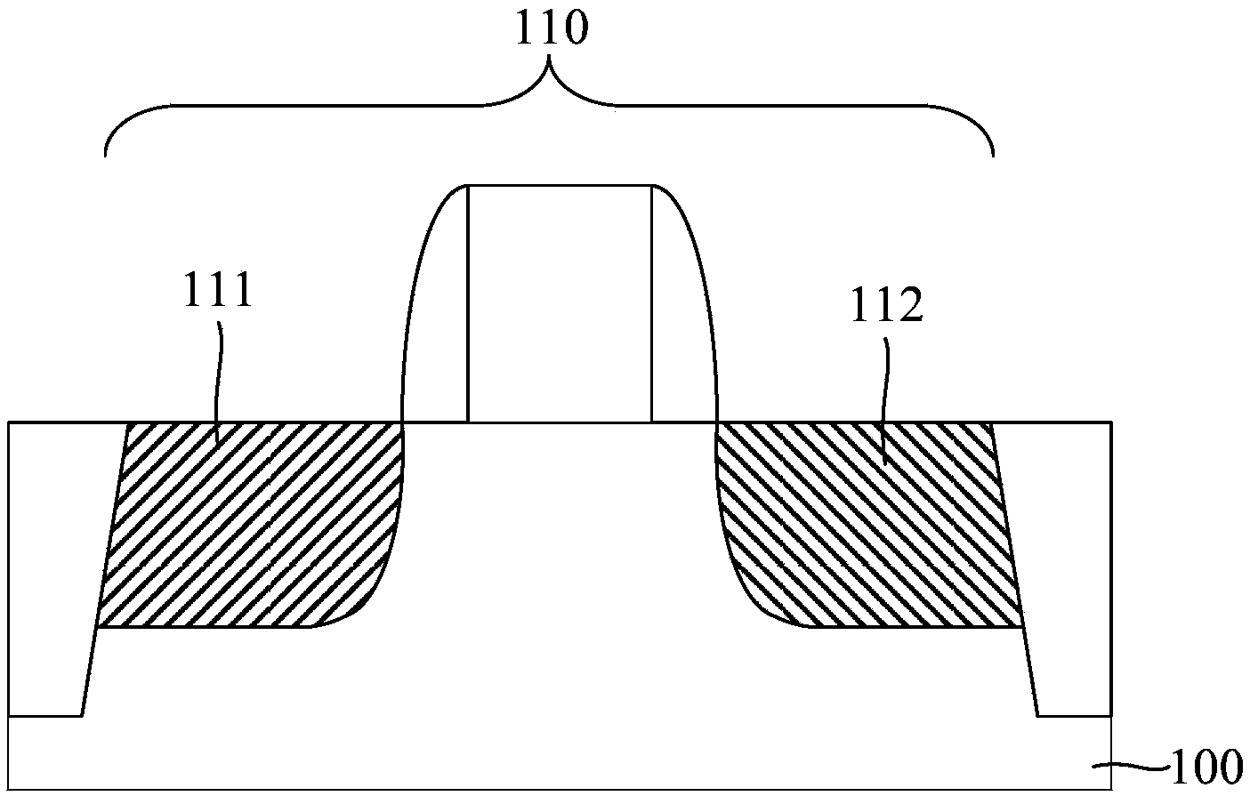
[0055] providing a substrate (corresponding to the base in the semiconductor processing process), on which a groove is etched in the part where the source and drain regions are to be formed;
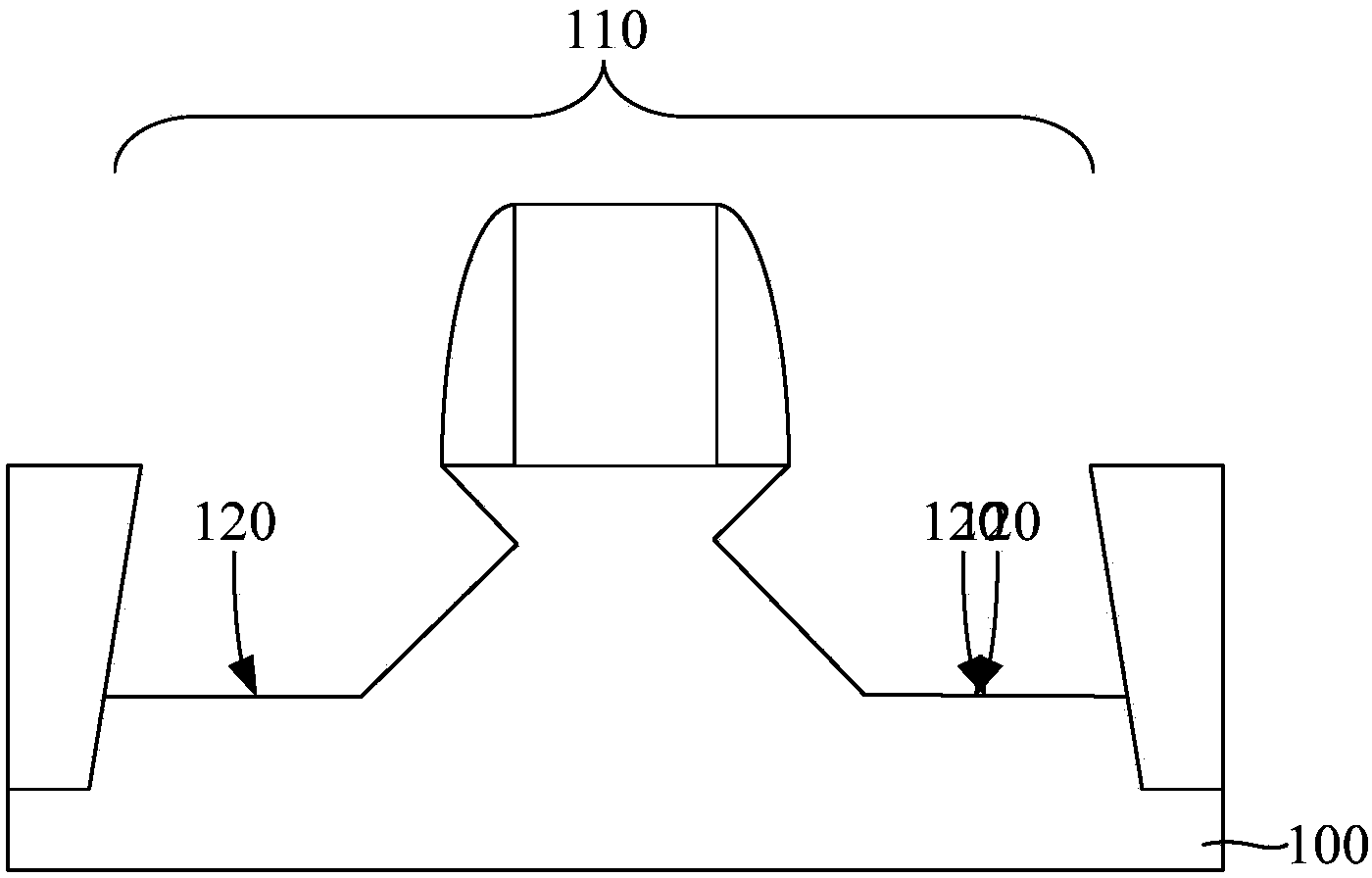
[0056] performing at least one oxidation-deoxidation treatment on the groove;
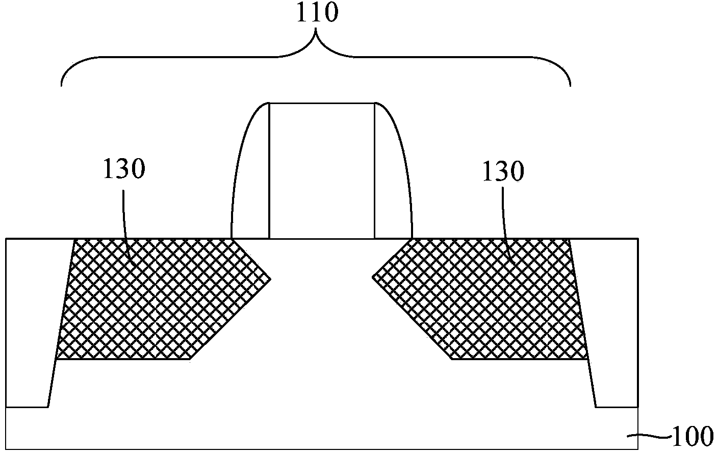
[0057] forming a strain-inducing layer in the groove; wherein,
[0058] Described oxidation-reoxidation treatment comprises:
[0059] Oxidizing the surface of the groove to form an oxide layer on the surface of the groove;
Login to View More PUM
 Abstract
The invention discloses a semiconductor treatment technology. The semiconductor treatment technology includes the step of providing a substrate and carrying out oxidation and oxidation layer removing treatment on the substrate at least once, wherein the oxidation and oxidation layer removing treatment includes the first step of carrying out oxidation treatment on the surface of the substrate and forming an oxidation layer on the surface of the substrate, and the second step of removing the oxidation layer and exposing the substrate. The invention further provides a semiconductor device preparation method through the semiconductor treatment technology so as to improve the performance of an embedded silicon germanium device. Through the oxidation and oxidation layer removing treatment, defects on the surface of the substrate can be reduced or eliminated, so the surface of the substrate is smooth and is beneficial for the next procedure.
Description
technical field [0001] The invention relates to the technical field of semiconductor manufacturing, in particular to a semiconductor processing technology and a method for preparing a semiconductor device. Background technique [0002] The fabrication of large scale integrated circuits requires a supply of large numbers of transistor elements representing the main circuit elements used to design circuits. Among them, for complex circuits (such as microprocessors, storage chips, etc.), because CMOS technology has superior characteristics of operating speed, power consumption, and cost-effectiveness, CMOS (complementary metal oxide semiconductors, including P-channel transistors and N Trench transistor, namely PMOS and NOMS) technology is currently the most promising approach. Whether it is an N-channel transistor or a P-channel transistor, it includes a PN junction through a highly doped drain region and a source region and a reverse electrode disposed between the drain regi...
Claims
Login to View More Application Information
Patent Timeline
 Patent Type & AuthorityApplications(China)
IPC IPC(8): H01L21/336H01L21/322
CPCH01L21/02381H01L21/0243H01L21/02532H01L29/66568H01L21/02639H01L21/02057H01L21/02252H01L21/302H01L21/3065H01L21/31116H01L29/66636H01L29/7848H01L29/165H01L21/02238H01L21/76205
Inventor李全波黄君孟祥国张瑜
OwnerSHANGHAI HUALI MICROELECTRONICS CORP