

Parameter sending method of storage chip of imaging box, storage chip and imaging box
A storage chip and transmission method technology, which is applied in the fields of electronic digital data processing, visual representation of photographic printing, permanent visual display devices, etc.
- Summary
- Abstract
- Description
- Claims
- Application Information
AI Technical Summary
Problems solved by technology
Method used
Image

Examples
Embodiment 1
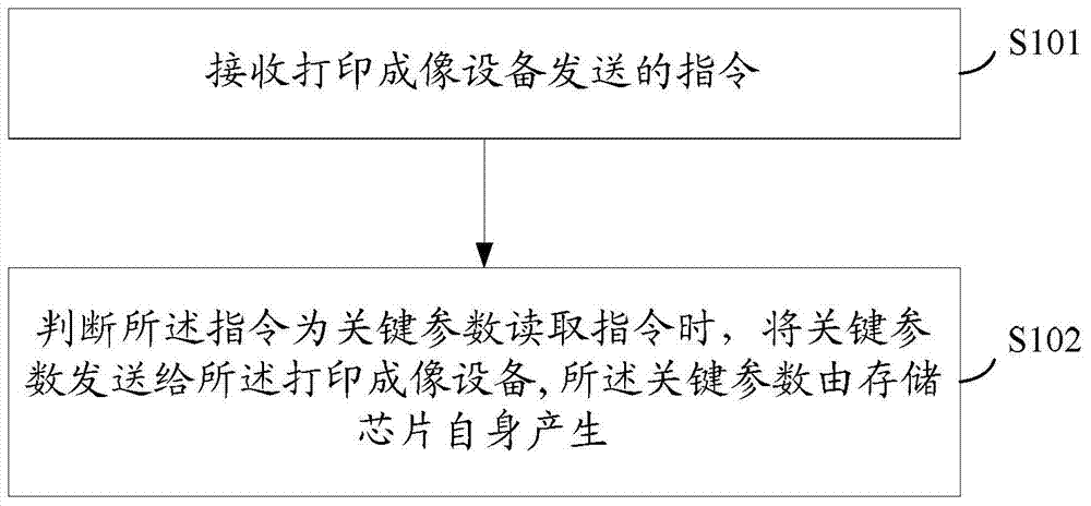
[0073] see figure 1 , which is a flow chart of Embodiment 1 of the method for sending parameters of the memory chip of the imaging box provided by the present invention.
[0074] The method for sending parameters of the memory chip of the imaging box provided in this embodiment includes the following steps:
[0075] S101: Receive an instruction sent by a printing and imaging device;
[0076] It should be noted that the instructions sent by the printing and imaging device to the storage chip of the imaging box may include reading instructions and other types of instructions. The reading instruction refers to the need to read certain parameters from the storage chip to the printing and imaging device .
[0077] Of course, it can be understood that some instruction types do not need to read parameters from the memory chip to the printing and imaging device.
[0078] S102: When it is judged that the instruction is a key parameter reading instruction, send the key parameter to t...
Embodiment 2
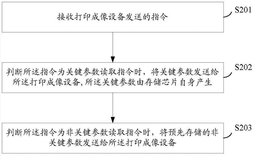
[0084] see figure 2 , which is a flow chart of Embodiment 2 of the method for sending parameters of the memory chip of the imaging box provided by the present invention.
[0085] S201: Receive an instruction sent by a printing and imaging device;
[0086] S202: When it is judged that the instruction is a key parameter reading instruction, send the key parameter to the printing and imaging device, and the key parameter is generated by the memory chip itself.
[0087] S201 and S202 are the same as S101-S102 in the first method embodiment, and will not be repeated here.
[0088] S203: When it is judged that the instruction is a non-critical parameter reading instruction, send the pre-stored non-critical parameter to the printing and imaging device.
[0089] The non-critical parameters are parameters pre-stored by the memory chip.
[0090] It should be noted that non-key parameters can still be stored in the memory chip. These non-key parameters can be read directly and do not...
Embodiment 3
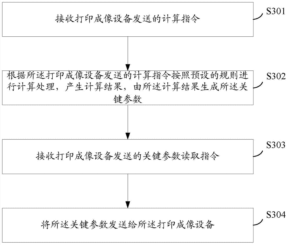
[0092] see image 3 , which is a flow chart of Embodiment 3 of the parameter sending method of the memory chip of the imaging box provided by the present invention.
[0093] It should be noted that both the key parameter read instruction and the non-key parameter read instruction belong to the read instruction. In addition to the read instruction, it may also include a calculation instruction. The calculation instruction in this embodiment is the key parameter generated by the memory chip itself. One of the calculation conditions for parameters, the calculation instructions referred to in the present invention are not the instructions defined by the printing imaging device for instructing the storage chip to perform calculations, but the instructions defined by the storage chip for all instructions that can be used to generate calculation results. Collectively, it may include the above-mentioned key parameter reading instructions and non-key parameter reading instructions. Th...
PUM
 Abstract
Description
Claims
Application Information