
Method for doping of different-valence metal ions in semiconductor

A metal ion and semiconductor technology, which is applied in the field of heterovalent metal ion doping, can solve the problems of difficult doping, weak light emission from doping, etc., and achieves the effects of simple device and low cost

Active Publication Date: 2014-06-25
BEIJING INSTITUTE OF TECHNOLOGYGY
View PDF3 Cites 9 Cited by
  • Summary
  • Abstract
  • Description
  • Claims
  • Application Information

AI Technical Summary

Problems solved by technology

In 2006, Dalpian GM and others found that the smaller the volume of nanocrystals, the deeper the energy level of impurities, the greater the energy required for doping, and the more difficult the doping, resulting in the "self-purification" of nanocrystals that are difficult to dope (Self -purification) problem
However, most of the current reports are doped with weak luminescence

Method used


Image

  • Method for doping of different-valence metal ions in semiconductor
  • Method for doping of different-valence metal ions in semiconductor
  • Method for doping of different-valence metal ions in semiconductor

Examples


preparation example Construction

[0040] The preparation method of the precursor solution of sulfur is as follows:

[0041] Take 5ml of oleylamine and 10ml of oleic acid, add them to a 50ml round bottom flask in sequence, stir evenly, weigh 64mg of sulfur powder, add it to the above mixture, stir at room temperature for 2min, and react with magnetic stirring in an oil bath at 100°C for 40min, and pour into it 15ml of toluene was added, magnetically stirred evenly, and the temperature was lowered to room temperature to obtain a sulfur precursor solution.

[0042] The preparation method of the precursor solution of selenium is as follows:

[0043] Take 6-10ml of octadecene (ODE) in a three-necked flask, weigh 79mg of selenium powder into the above-mentioned three-necked flask, stir evenly with a magnetic force, heat to 270-300°C in a constant temperature heating mantle, and stir the reaction at this temperature for 15min to Form a yellow transparent clear solution, stop heating, cool down to room temperature, a...

Embodiment 1

[0052] (1) Take 6ml of monodisperse 4nmAg toluene sol in a 25ml round bottom flask, add 3ml of sulfur precursor solution to it, stir and react in a water bath at 50°C for 1h, add ethanol, and centrifuge at 5000r for 8min to obtain monodisperse Ag 2 S nanoparticles, redispersed in 6-10ml toluene to obtain Ag 2 S nanoparticle sol.

[0053] (2) The monodisperse Ag obtained in step (1) 2 S nanoparticle sol, under magnetic stirring, add 0.2ml oleic acid, 0.1ml oleylamine and 1ml Cd(NO 3 ) 2 4H 2 O methanol solution (0.1g / ml), magnetically stirred at room temperature for 1min, added 0.1ml TBP, reacted with magnetically stirred in a water bath at 50°C for 2h, added ethanol, centrifuged at 5000r for 8min, and obtained CdS quantum dots with 1% silver doping (1% is atomic proportion).

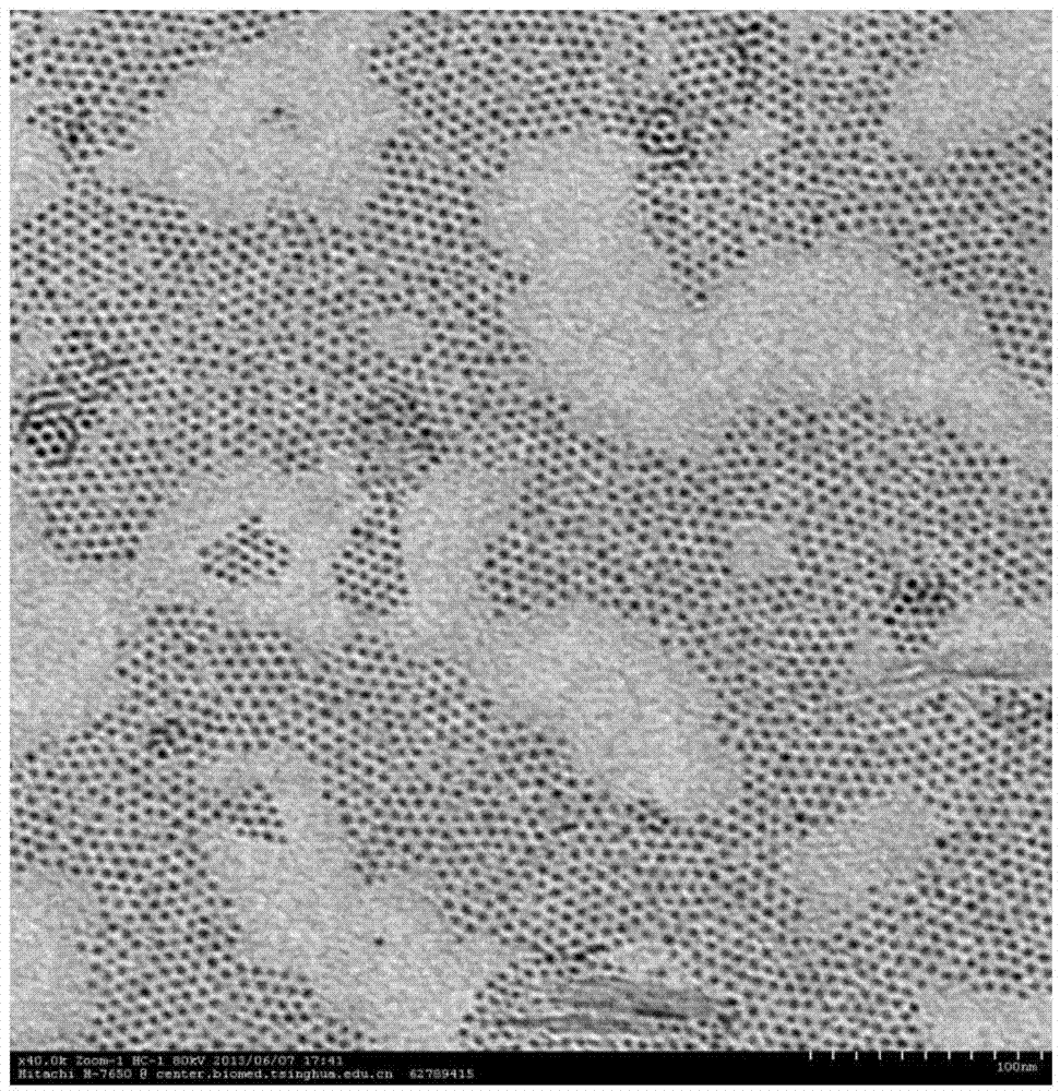
[0054] The resulting CdS quantum dots were detected by transmission electron microscopy, showing that they had good monodispersity (e.g. figure 1 shown), the size of a single CdS nanoparticle is a...

Embodiment 2

[0056] (1) Take 6ml of monodisperse 4nmAg toluene sol in a 25ml round bottom flask, add 3ml of sulfur precursor solution to it, stir and react in a water bath at 50°C for 1h, add ethanol, and centrifuge at 5000r for 8min to obtain monodisperse Ag 2 S nanoparticles, redispersed in 6-10ml toluene to obtain Ag 2 S nanoparticle sol.

[0057] (2) The monodisperse Ag obtained in step (1) 2 S nanoparticle sol, under magnetic stirring, add 0.2ml oleic acid, 0.1ml oleylamine and 1ml Cd(NO 3 ) 2 4H 2 O methanol solution (0.1g / ml), magnetically stirred at room temperature for 1min, added 0.2ml TBP, reacted with magnetically stirred in a water bath at 50°C for 2h, added ethanol, centrifuged at 5000r for 8min, and obtained CdS quantum dots with 1% silver doping (1% is atomic proportion).


PUM


Abstract

The invention relates to a method for doping of different-valence metal ions in a semiconductor, and belongs to the field of green preparation of semiconductor nano-materials and photoelectric performance regulation. The method comprises the steps that oleic acid and oleylamine are added to nano-particle sol of a chalcogen compound MxXy of different-valence metal M, and stirring is carried out evenly to obtain a mixture a; a methanol solution of cadmium salt is then added to the mixture a, and stirring is carried out evenly to obtain a mixture b; phosphine ligand is added to the mixture b, stirring and reaction are carried out at 30 DEG C to 80 DEG C for two hours to four hours, washing and centrifuging are carried out to obtain sediment c, the obtained sediment c is dispersed in a non-polarity organic solvent, and a different-valence doped semiconductor is obtained. The method is simple in operation, effective substituting doping of the different-valence metal ions in the semiconductor photoelectric nano-materials is achieved in the solvent at low temperature, the luminance on the semiconductor nano-materials and regulation of p-type and n-type conduction types are achieved, and application fields are wide.

Description

technical field [0001] The invention relates to a method for doping asymmetric metal ions in semiconductors, and belongs to the field of green preparation and photoelectric performance regulation of semiconductor nanometer materials. Background technique [0002] Semiconductor nanocrystals have many unique properties, such as quantum size effects, quantum confinement effects, surface and interface effects, which are different from bulk materials, and have superior luminescence and photoelectric conversion properties. The energy band regulation of II-VI-based semiconductor nanocrystals and composite nanocrystals spans the entire range of ultraviolet, visible and near-infrared regions, and is an excellent light-emitting diode, high-mobility transistor, thermal / infrared detection, photoconductivity and solar cells. Material. The reason why semiconductors can be widely used in today's optoelectronic world is that implanting impurities in their crystal lattices can change their ...

Claims


Application Information

Patent Timeline
Patent Type & Authority Applications(China)
IPC IPC(8): H01L21/06
CPCB82Y30/00H01L21/06
Inventor 张加涛赵倩钱红梅桂晶
Owner BEIJING INSTITUTE OF TECHNOLOGYGY
Features
  • Generate Ideas
  • Intellectual Property
  • Life Sciences
  • Materials
  • Tech Scout
  • Unparalleled Data Quality
  • Higher Quality Content
  • 60% Fewer Hallucinations
Learn More